Spatially modulated detector for radiation

Inactive Publication Date: 2000-12-05
INTERUNIVERSITAIR MICRO ELECTRONICS CENT (IMEC VZW)
View PDF7 Cites 43 Cited by
  • Summary
  • Abstract
  • Description
  • Claims
  • Application Information

AI Technical Summary

Benefits of technology

It is a first aim of the present invention to provide a radiation detection device that allows detecting single cha

Problems solved by technology

This lowers system yield and adds significantly to the cost of the system.
Large numbers of detectors need to be connected to the CMOS circuitry, which is difficult to achieve.
However, it is known that light detection directly in CMOS yields low detector-response times. As stated by Levine et al. in "1 Gb/s Si high quantum efficiency monolithically integrable 880 nm detector", Applied Physics Letters vol.
A typical problem when using the neutral zone in the semiconductor substrate for constructin

Method used


Image

  • Spatially modulated detector for radiation
  • Spatially modulated detector for radiation
  • Spatially modulated detector for radiation

Examples


Embodiment Construction

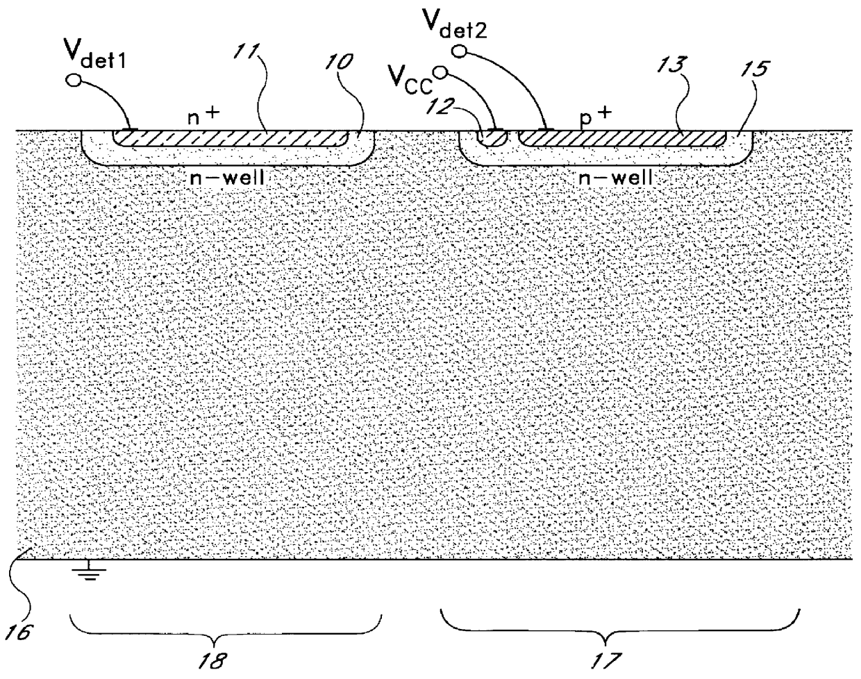
In the detailed description of the invention, the explanation is limited to light detection in chips made by a standard CMOS process with single N-well technology. With this description, the person skilled in the art can extend the use and the merits of the present invention to other technologies such as p-well, dual-well and BICMOS technologies. Several layouts and construction methods for a robust and fast substratedetector are included. The combination with image fibers delivers a system that is ideally suited for parallel optical interconnects.

To focus on the difficulties to detect light in standard CMOS, FIG. 1 is given. The construction of n-well, and highly doped n.sup.+ and p.sup.+ regions are included in the definition of the process. We assume the substrate to be lightly p-doped. Usually, the n.sup.+ -regions serve as drain and source regions for the NMOS transistors, and as strap to contact n-wells. Conversely, the p.sup.30 -regions usually serve as drain and source for t...


PUM


Abstract

A novel radiation detector, a detection principle and an associated structure are provided for semiconductor substrate detectors in general and for CMOS based circuits in particular. For an optical detector, photons absorbed in the neutral zone of the substrate generate electron hole pairs that migrate by diffusion. A shadow mask gives a spatial modulation to the incident, and consequently, to the absorbed light in the semiconductor substrate. By measuring the magnitude of the spatial frequency component in the minority carrier distribution with a spatial frequency corresponding to that of the shadow mask, a fast detector is conceived. A shadow mask with higher spatial modulation frequency delivers a faster turn-off. The combination of a plurality of these detectors with an image fiber forms a basic system for constructing high-speed parallel optical interconnects between chips.

Description

1. Field of the InventionThe invention relates to the field of detection of radiation in a semiconductor substrate. More in particular, the present invention is related to a time-differentiated measurement of the spatial modulation of carriers generated by radiation and diffusing in the substrate.2. Description of the Related ArtDevices receiving light at high speed in specially conceived receiver photo-diodes constructed in, for example, silicon or in III-V semiconductor material arc known in the art. The acquired information stream is often further processed or used in CMOS or BICMOS circuitry. This approach requires hybridization of the receiver (or of the receiver diodes) with the CMOS (or BICMOS) circuitry. This lowers system yield and adds significantly to the cost of the system. When constructing, for example, parallel optical interconnects between CMOS circuits, there is a need for light sources and for light detectors. Large numbers of detectors need to be connected to the ...

Claims


Application Information

Patent Timeline
IPC IPC(8): H01L27/144G01J1/02
CPCH01L27/1443
Inventor KUIJK, MAARTENHEREMANS, PAULCOPPEE, DANIELVOUNCKX, ROGER
Owner INTERUNIVERSITAIR MICRO ELECTRONICS CENT (IMEC VZW)
Why Eureka
Try Eureka