Semiconductor device featuring copper wiring layers of different widths having metal capping layers of different thickness formed thereon, and method for manufacturing the same

Inactive Publication Date: 2006-07-20
RENESAS ELECTRONICS CORP
View PDF4 Cites 43 Cited by
  • Summary
  • Abstract
  • Description
  • Claims
  • Application Information

AI Technical Summary

Benefits of technology

[0012] Therefore, an object of the present invention is to provide a semiconductor device which is constituted such that not only can both an anti-electromigration cha

Problems solved by technology

With the advance of miniaturization and integration of semiconductor devices, the wiring pattern layers become smaller, and thus the signal lines become narrower, resulting in delay of signal propagation in the narrowed wiring lines, due to a parasitic resistance of the signal lines themselves and a parasitic capacitance involved in the signal lines.
Also, as a problem peculiar to fine copper wiring layers, there is a stress induced voiding (SIV) problem, in which voids are produced in roots of the

Method used


Image

  • Semiconductor device featuring copper wiring layers of different widths having metal capping layers of different thickness formed thereon, and method for manufacturing the same
  • Semiconductor device featuring copper wiring layers of different widths having metal capping layers of different thickness formed thereon, and method for manufacturing the same
  • Semiconductor device featuring copper wiring layers of different widths having metal capping layers of different thickness formed thereon, and method for manufacturing the same

Examples


first embodiment

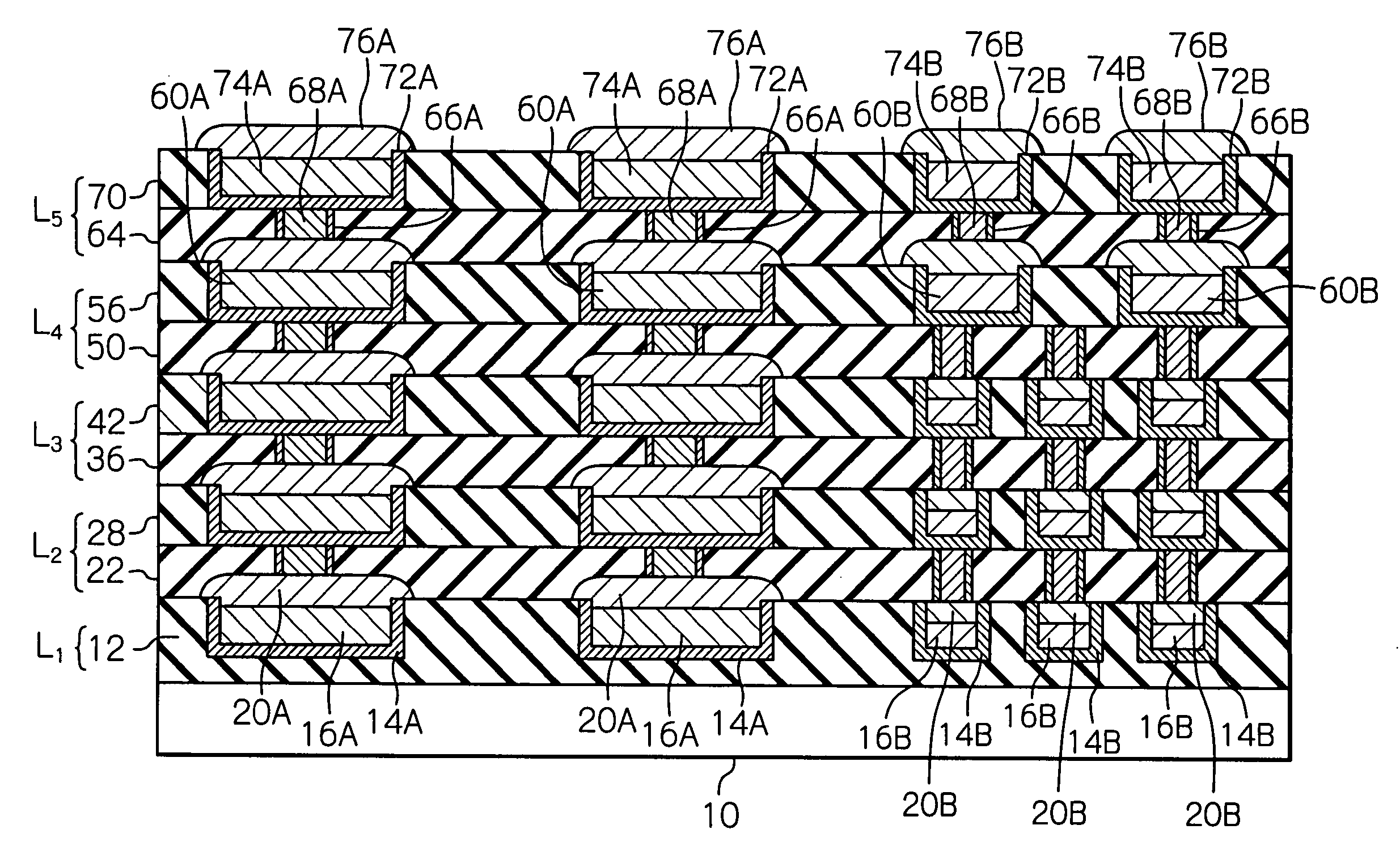
[0048] With reference to FIGS. 2A to 20, the method for manufacturing a semiconductor device according to the present invention is explained below.

[0049] First, referring to FIG. 2A, as a similar way to the case of FIG. 1A, reference 10 indicates a semiconductor substrate, which may be formed as a silicon substrate. Also, various semiconductor elements (not shown), such as transistors, resistors, capacitors and so on, are produced in advance in the semiconductor substrate 10, using various well-known processes.

[0050] After the production of the semiconductor elements in the semiconductor substrate 10 is completed, an insulating layer 12 (i.e., an insulating interlayer L1) is formed as a silicon dioxide layer on the semiconductor substrate 10 by a suitable CVD process, and a plurality of wide trenches 12A and a plurality of narrow trenches 12B are formed in the insulating interlayer 12, using a photolithography and etching process. The wide trenches 12A are arranged at a given pitch...

second embodiment

[0101] With reference to FIGS. 3A to 3H, the method for manufacturing a semiconductor device according to the present invention is explained below.

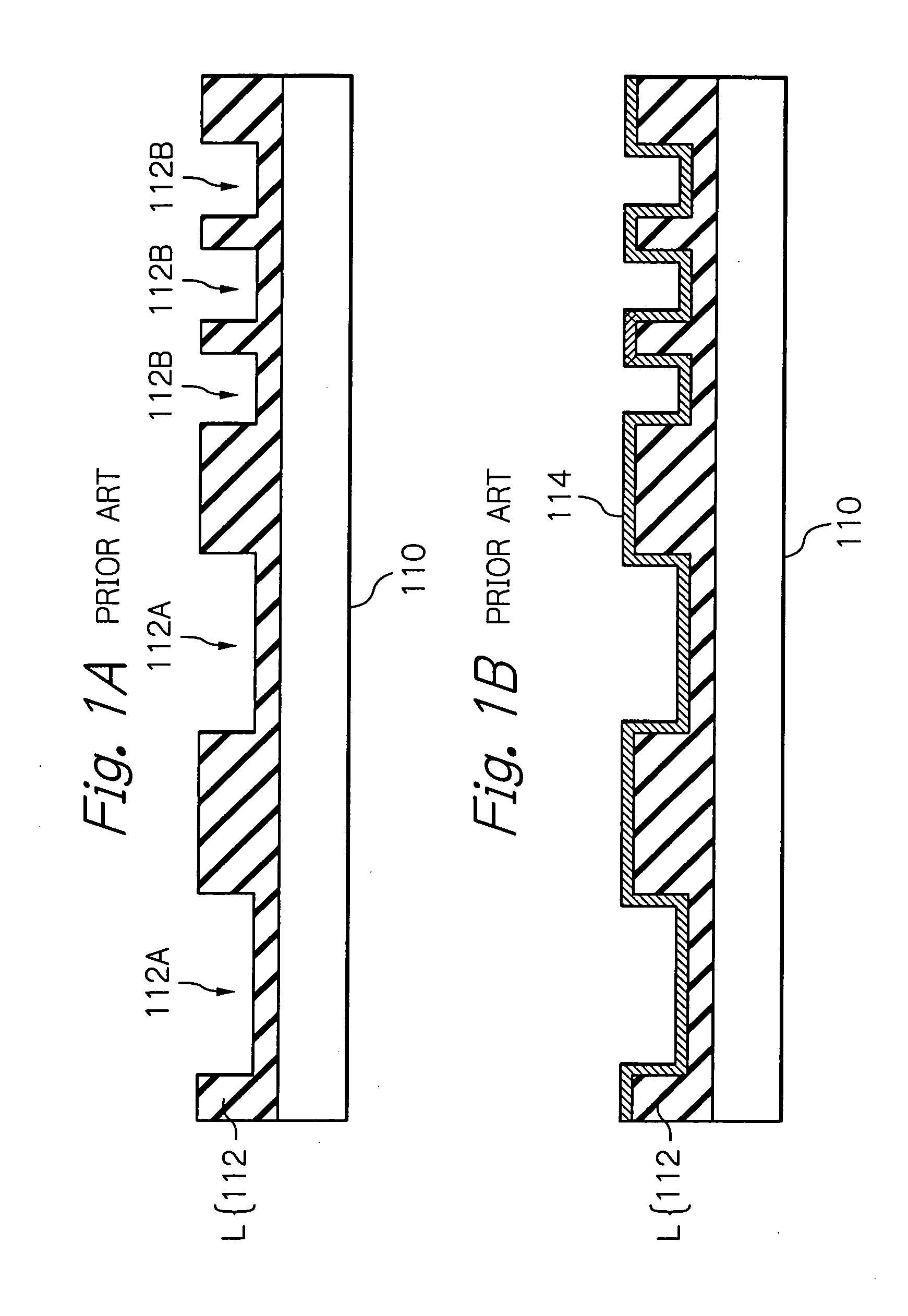
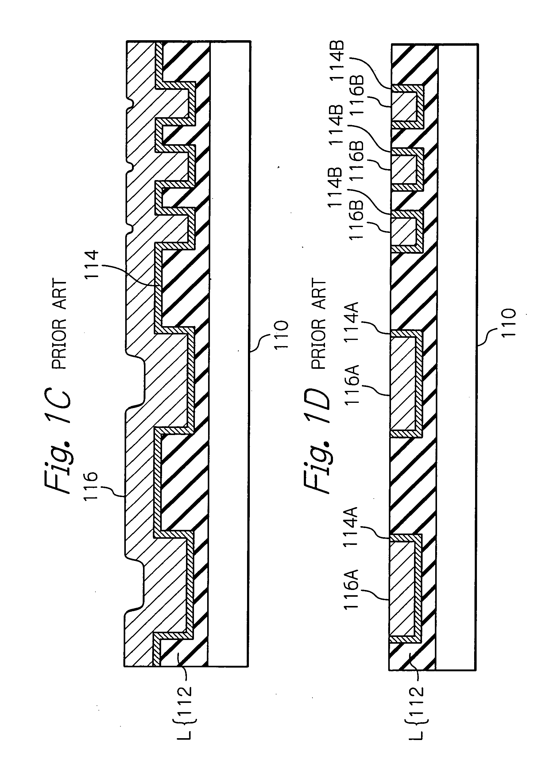
[0102] As stated with reference to FIG. 2B, in the aforesaid first embodiment, the metal barrier layer 14A is formed as the semi-amorphous layer in which tantalum nitride (TaN) is amorphous and tantalum (Ta) is crystallized. As a result, in FIGS. 2C and 2D, there may be a case where both the Cu layers 16A1 and 16A2 are formed as a semi-amorphous copper (Cu) layer in the wide trenches 12A. The second embodiment is directed to how the semi-amorphous copper (Cu) layer (16A1 and 16A2) is processed.

[0103] Referring to FIG. 3A which corresponds to FIG. 2D, the semi-amorphous Cu layer (16A1 and 16A2) includes a plurality of crystallized copper (Cu) regions, one of which is representatively indicated by reference 161A. Similar to the crystallized Cu layer 16B1, with which the narrow trenches 14B are filled, the crystallized Cu region 161A has a ...

third embodiment

[0118] With reference to FIGS. 5A, 5B and 5C, the method for manufacturing a semiconductor device according to the present invention is explained below.

[0119] Similar to the aforesaid second embodiment, in this third embodiment, both the Cu layers 16A1 and 16A2 are formed as a semi-amorphous copper (Cu) layer in the wide trenches 12A, and the third embodiment is also directed to how the semi-amorphous copper (Cu) layer (16A1 and 16A2) is processed.

[0120] First, referring to FIG. 5A which corresponds to FIG. 3F, similar to the aforesaid second embodiment, the CoWP electroplating process is continued until the Cu2O layer 181A and 18B (see: FIG. 3C) are removed from the Cu region 161A and narrow Cu wiring layers 16B, to thereby form the respective CoWP capping layers 20A on the wide Cu wiring layers 16A. Then, the CoWP electroplating process is stopped, and the semiconductor substrate 10 is taken out of the CoWP electroplating solution containing the Cu2O removal agent.

[0121] Next, r...


PUM


Abstract

In a semiconductor device, an insulating interlayer is provided above a semiconductor substrate, and a plurality of first wiring layers and a plurality of second wiring layers are formed in the insulating interlayer. The first wiring layers are substantially composed of copper, and are arranged in parallel at a large pitch. The second wiring layers are substantially composed of copper, and are arranged in parallel at a small pitch. A first metal capping layer is formed on each of the first wiring layers, and a second metal capping layer is formed on each of the second wiring layers. The second metal capping layer has a smaller thickness than that of the first metal capping layer.

Description

BACKGROUND OF THE INVENTION [0001] 1. Field of the Invention [0002] The present invention relates to a semiconductor device which features copper wiring layers having metal capping layers formed thereon, and a method for manufacturing such a semiconductor device. [0003] 2. Description of the Related Art [0004] In a process of production of semiconductor devices, semiconductor elements, such as transistors, resistors, capacitors and so on, are produced in a semiconductor substrate, and then a multi-layered wiring structure is formed on the semiconductor substrate. The multi-layered wiring structure includes a local multi-layered wiring section formed on the semiconductor substrate, and a global multi-layered wiring section formed on the local multi-layered wiring section. [0005] The local multi-layered wiring section includes a plurality of insulating interlayers, a plurality of wiring pattern layers each formed on one of the insulating interlayers, a plurality of groups of via plugs...

Claims


Application Information

Patent Timeline
IPC IPC(8): H01L23/52
CPCH01L21/2885H01L21/76843H01L21/76849H01L21/76877H01L23/53238Y10S438/978H01L2924/0002H01L2924/00
Inventor TAKEWAKI, TOSHIYUKIUENO, KAZUYOSHI
Owner RENESAS ELECTRONICS CORP
Why Eureka
Try Eureka