Non-volatile memory resistor cell with nanotip electrode

a memory resistor and nanotip electrode technology, applied in the field of integrated circuit (ic) fabrication, can solve the problems that sram and dram memories cannot retain stored information, require extra fabrication processes, etc., and achieve the effect of promoting bipolar switching characteristics

Inactive Publication Date: 2006-07-20
SHARP KK
View PDF13 Cites 118 Cited by
  • Summary
  • Abstract
  • Description
  • Claims
  • Application Information

AI Technical Summary

Benefits of technology

[0015] The present application describes a memory resistor cell where one of the electrodes is formed with nanotips extending into the memory resistor material. The conductive nanotips create an asymmetric electrode structure that creates non-u...

Problems solved by technology

SRAM and DRAM memories cannot retain the stored information without a p...

Method used


Image

  • Non-volatile memory resistor cell with nanotip electrode
  • Non-volatile memory resistor cell with nanotip electrode
  • Non-volatile memory resistor cell with nanotip electrode

Examples


Embodiment Construction

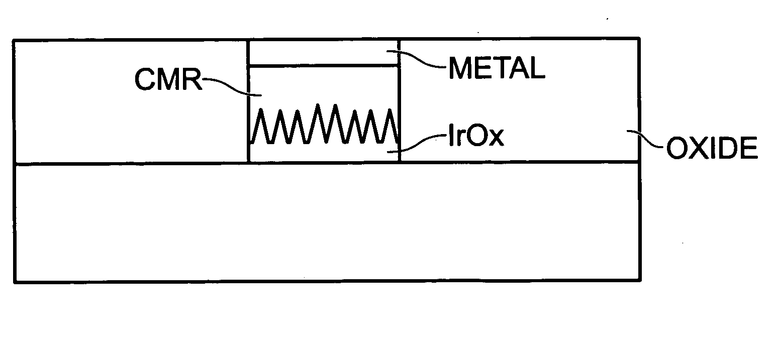
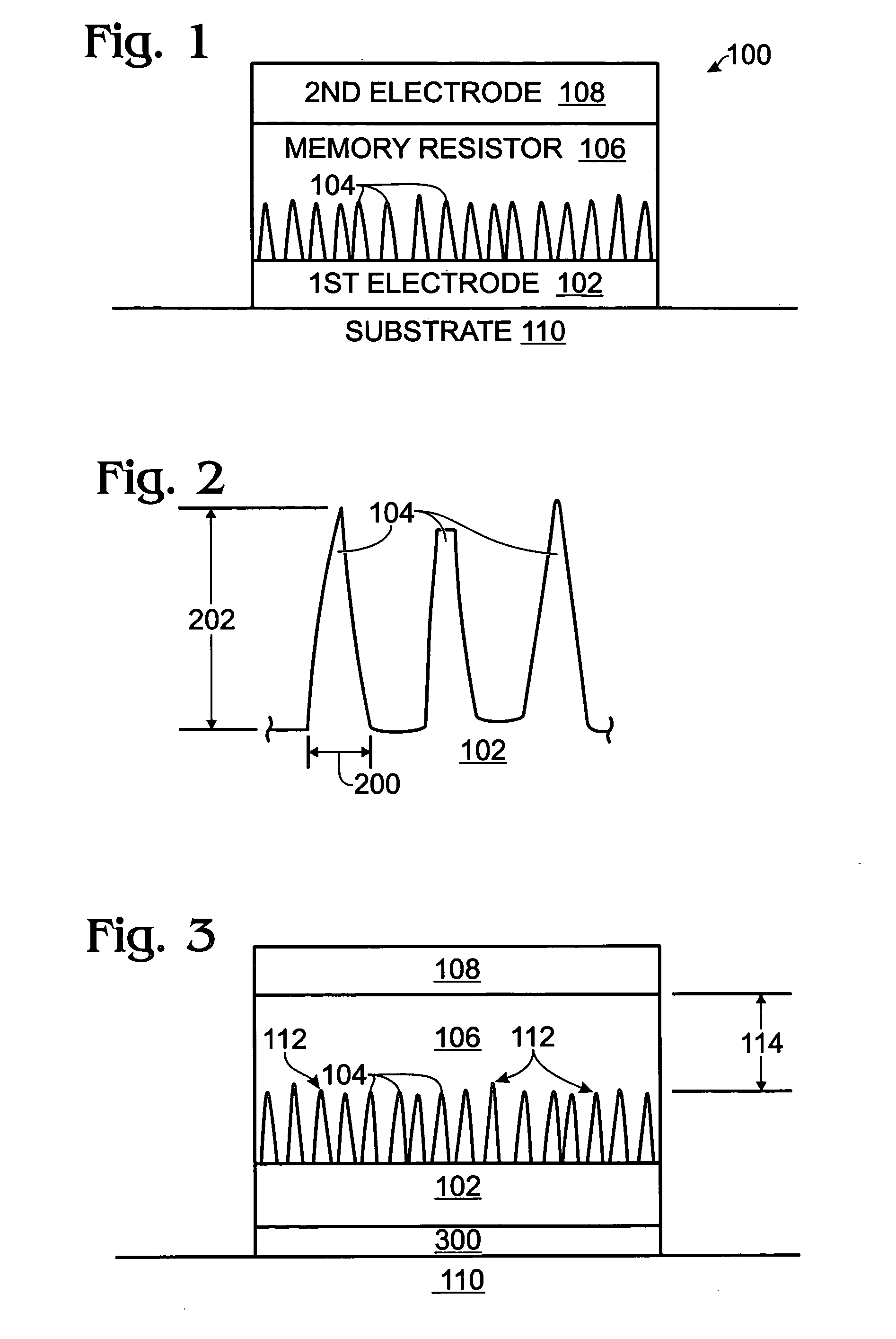
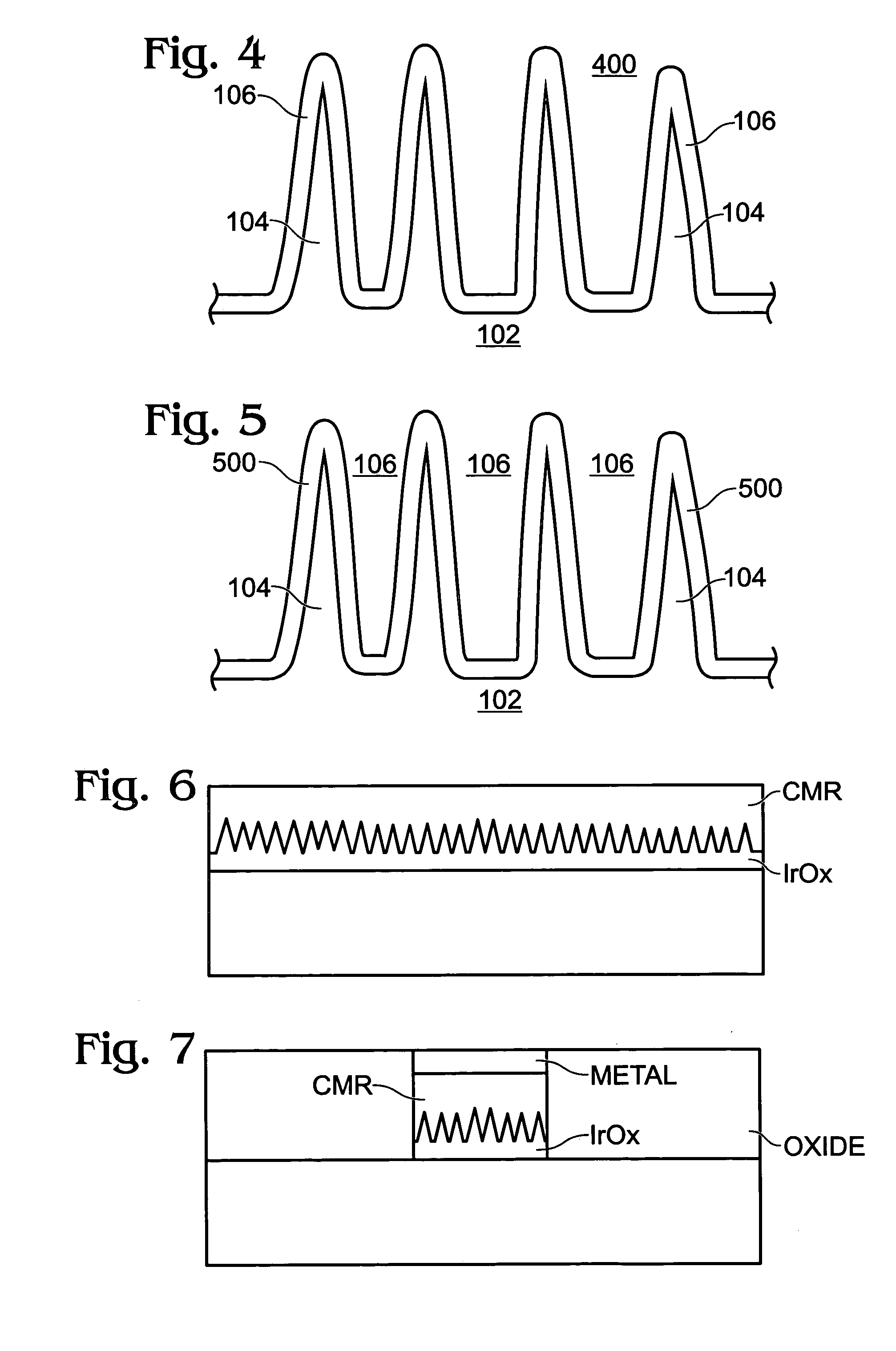
[0030]FIG. 1 is a partial cross-sectional view of a nanotip electrode non-volatile memory resistor cell. The memory cell 100 comprises a first electrode 102 with nanotips 104. A memory resistor material 106 is adjacent the nanotips 104. A second electrode 108 is adjacent the memory resistor material 106. More specifically, the memory resistor material 106 is interposed between the first electrode 102 and second electrode 108. A number of different arrangements of memory resistor material are possible. Generally, the memory resistor material 106 may be on the nanotips 104, surrounding and on the nanotips, and between and on the nanotips. The arrangement shown in FIG. 1 satisfies all these descriptions, but other variations of the cell 100 are presented below.

[0031] As used herein, the word “nanotip” is not intended to be limited to any particular physical characteristics, shapes, or dimensions. The nanotips may alternately be known as nanorods, nanotubes, or nanowires. In some aspec...


PUM


Abstract

A non-volatile memory resistor cell with a nanotip electrode, and corresponding fabrication method are provided. The method comprises: forming a first electrode with nanotips; forming a memory resistor material adjacent the nanotips; and, forming a second electrode adjacent the memory resistor material, where the memory resistor material is interposed between the first and second electrodes. Typically, the nanotips are iridium oxide (IrOx) and have a tip base size of about 50 nanometers, or less, a tip height in the range of 5 to 50 nm, and a nanotip density of greater than 100 nanotips per square micrometer. In one aspect, the substrate material can be silicon, silicon oxide, silicon nitride, or a noble metal. A metalorganic chemical vapor deposition (MOCVD) process is used to deposit Ir. The IrOx nanotips are grown from the deposited Ir.

Description

BACKGROUND OF THE INVENTION [0001] 1. Field of the Invention [0002] This invention generally relates to integrated circuit (IC) fabrication and, more particularly, to a memory resistor cell made using an electrode with nanotips. [0003] 2. Description of the Related Art [0004] Semiconductor IC memory devices have replaced magnetic-core memory devices, as IC devices have lower fabrications cost and exhibit higher performance. An IC memory circuit includes a repeated array of memory cells, each of which stores one state of a two-state information (0 or 1), or multi-state information (for example, 00, 01, 10, or 11 of 4 states). This array of cells works together with support circuitry such as a row decoder, a column decoder, a write circuit to write to the memory cell array, a control circuitry to select the correct memory cell, and a sense amplifier to amplify the signal. [0005] One conventional memory circuit, the flip-flop, has an output that is stable for only one of two possible v...

Claims


Application Information

Patent Timeline
IPC IPC(8): H01L21/336
CPCH01L27/101H01L45/1273H01L45/16H01L45/1675H01L45/04H01L45/1233H01L45/147H10N70/8418H10N70/20H10N70/826H10N70/8836H10N70/011H10N70/063
Inventor HSU, SHENG TENGZHANG, FENGYANSTECKER, GREGORY M.BARROWCLIFF, ROBERT A.
Owner SHARP KK
Why Eureka
Try Eureka