Eureka AIR delivers breakthrough ideas for toughest innovation challenges, trusted by R&D personnel around the world.

Method for manufacturing semiconductor device

Active Publication Date: 2006-07-20
PANASONIC SEMICON SOLUTIONS CO LTD
View PDF1 Cites 7 Cited by
  • Summary
  • Abstract
  • Description
  • Claims
  • Application Information

AI Technical Summary

Benefits of technology

[0007] An object of the present invention is to provide a method for manufacturing a semiconductor device which allows a process control taking account of wafer information to be performed and which is capable of dealing with the process control in which a recipe is changed from one wafer to another.
[0009] According to such a configuration, unlike the conventional process techniques, the process control system does not belong to the manufacturing execution system (MES) and hence, the process control system is able to execute the process control independently. Because of this, it becomes possible to eliminate a time period during which the MES inquires a process control method of the process control system. Besides, since the step of acquiring a process result on a lot effected at the previous step as wafer information is included, it is possible to calculate a control parameter taking account of the states of wafers, thereby the process control can be performed from one wafer to another.
[0014] According to such a configuration, it is possible to handle even a lot of semiconductor device manufactured at faster than normal speed. That is, although there are cases where data on a lot is not yet sent when the process control system obtains a process result on the lot effected at a previous step from the database, processing on the lot can be performed by directly transmitting its data from the inspection apparatus to the process control system.
[0016] According to this configuration, it is possible to update the control parameter value at all times. Because of this, process control can be performed even on various types of semiconductor devices with high precision.

Problems solved by technology

In conventional process control techniques, since the manufacturing execution system (MES) inquires of its associated system the process control method, a problem has arisen in that it is difficult to use a manufacturing method in which the process control is performed from one wafer to another.
Also, another problem has arisen in that such a conventional system cannot handle process control which covers consecutive process steps, that is, process control which is performed based on a result effected at the next previous process step.

Method used


Image

  • Method for manufacturing semiconductor device
  • Method for manufacturing semiconductor device
  • Method for manufacturing semiconductor device

Examples


first embodiment

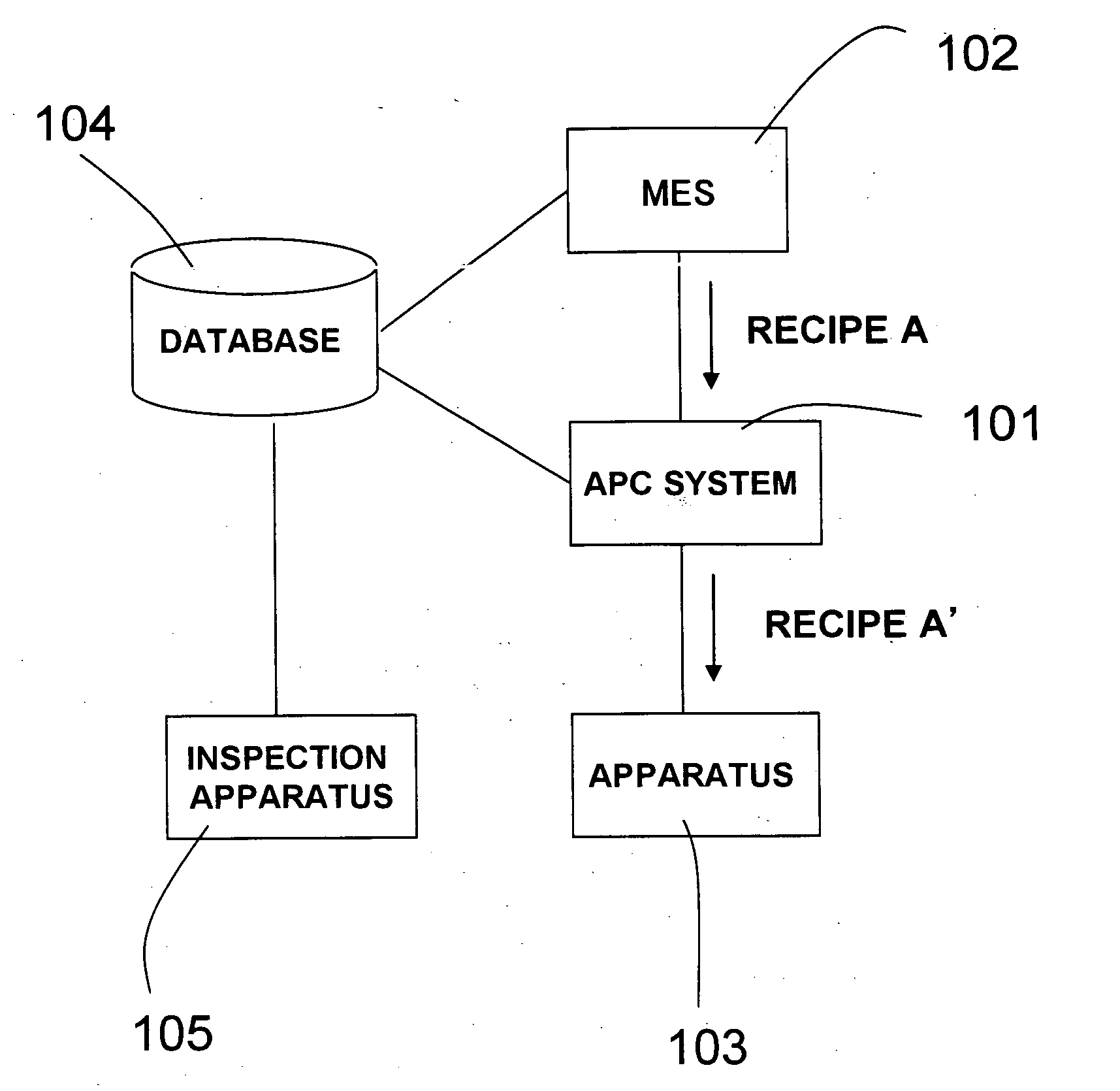
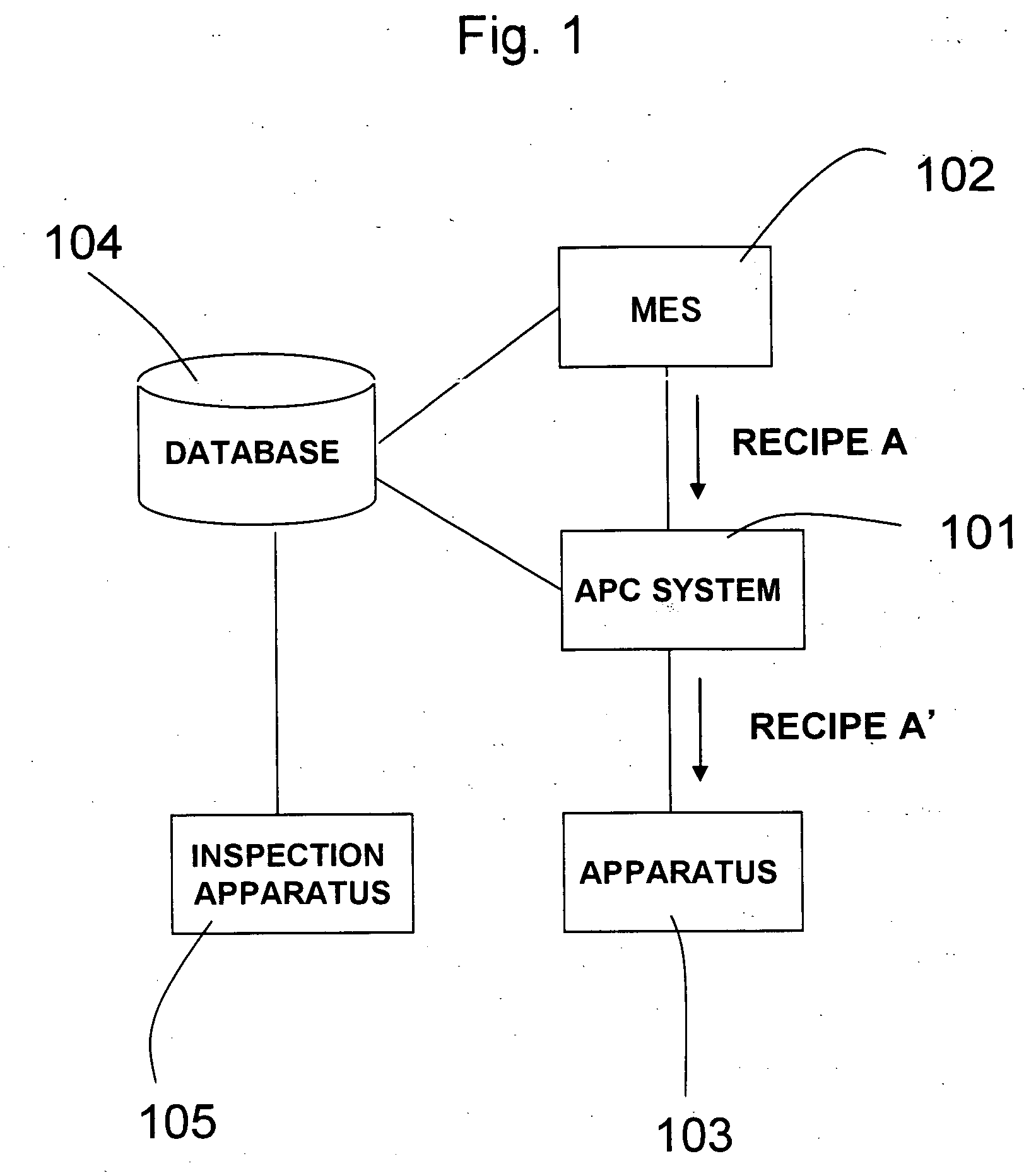
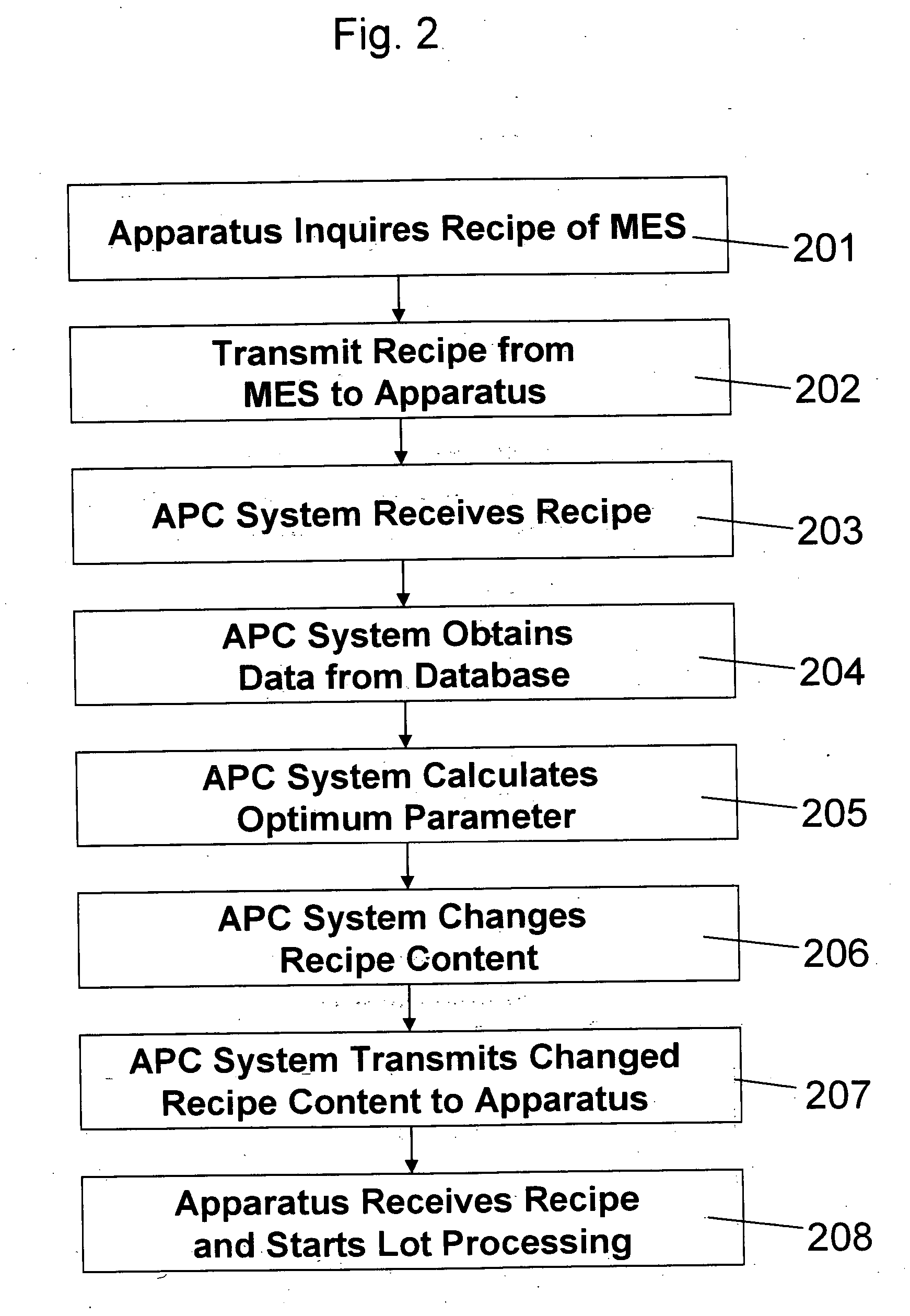
[0028] A first embodiment according to the present invention will be described with reference to FIGS. 1 to 4. FIG. 1 is a drawing for explaining a system configuration which includes an APC (advanced process control) system used in the invention.

[0029] As shown in FIG. 1, to transmit a process recipe from a manufacturing execution system 102 to a manufacturing apparatus 103 to conduct processing on a lot of semiconductor devices, a method for manufacturing a semiconductor device according to the first embodiment of the invention includes steps of inserting a process control system 101 into the path of a network where the manufacturing execution system 102 and the manufacturing apparatus 103 are connected with each other by a LAN, acquiring a process result on the lot at a previous step by using the process control system 101 to rewrite the process recipe, and transmitting the rewritten process recipe from the process control system 101 to the manufacturing apparatus 103.

[0030] Thr...

second embodiment

[0041] the invention will be described below with reference to FIGS. 6 and 7.

[0042] If the inventors dare to pose a problem on the first embodiment, there is a fact that the state of the manufacturing apparatus according to the first embodiment is not taken into account. That is, there is the problem that when a changed recipe content is transmitted to the apparatus in an abnormal state, an objective processing result cannot be obtained. When the state of the apparatus is abnormal, there is a difference in the preacquired calibration data shown in FIG. 5. Extremely speaking, when the state of the apparatus is abnormal, an optimum process control cannot be performed with the value calculated by the APC system according to the first embodiment of the invention. In such a case, there is a need to restrict the operation of the APC system for the change of the recipe.

[0043]FIG. 6 is a drawing for explaining a system configuration necessary for the second embodiment of the invention. Inc...

third embodiment

[0048] the invention will be described below with reference to FIGS. 8 and 9.

[0049] When semiconductor devices have been manufactured according to the first and second embodiments of the invention, no problems have been encountered in the regular lot processing. However, in the manufacture of semiconductors, there are ranks in lot processing, that is, there are lots whose processing proceeds at normal speed and lots whose processing proceeds at faster than the normal speed. The latter lots are called rushing lots, and in the rushing lot processing, a problem has been encountered in that when the APC system obtains a process result on the lot at the next previous step from the database, data on the lot is not present. It has been newly found that such a problem occurs because the lot proceeds to the next step, i.e., the process control step before the data on the lot is stored in the database.

[0050] Therefore, in the third embodiment of the invention, when a rushing lot is dealt wit...


PUM


Abstract

A method for manufacturing a semiconductor device is provided in which it is possible to perform process control taking account of wafer information and to deal with the process control in which a recipe is change from one wafer to another. The method comprises steps of inserting a process control system into the path of a network where a manufacturing execution system (MES) and a manufacturing apparatus are connected with each other by using a LAN, obtaining a process result on the lot of the wafers at a previous step through the use of the process control system to rewrite the process recipe, and transmitting the rewritten process recipe from the process control system to the manufacturing apparatus. Since the method includes the step of obtaining the process result on the lot effected at the previous step as wafer information, it is possible to calculate a control parameter taking account of the state of the wafers. Also, since a process control (APC) system is inserted between the MES and the apparatus, there is no communication between the MES and the APC system, so that a communication burden is reduced, thereby the process control can be performed from one wafer to another.

Description

BACKGROUND OF THE INVENTION [0001] 1. Field of the Invention [0002] The present invention relates to a method for manufacturing a semiconductor device which involves a process control technique used in a process for particularly manufacturing a semiconductor device. [0003] 2. Background Art [0004] Conventional process control techniques are often used based on sensor-derived data such as gas pressure and RF power of the inside of an apparatus. Besides, process controls are often performed in lots. That is, processes are conducted in such a way that one recipe corresponds to one lot. Take a gate etching process for instance. The etching is performed by changing the contents of a recipe into an optimum setting parameter value based on the sensor values of an etching apparatus. When there is a deviation in a gas pressure, the etching is performed after adjusting the value of the gas pressure. As a result, it is possible to perform the etching taking account of a change in the state of ...

Claims


Application Information

Patent Timeline
IPC IPC(8): G06F19/00H01L21/02H01L21/3065
CPCG05B19/41835G05B2219/32057G05B2219/32058G05B2219/32096G05B2219/32135G05B2219/32198G05B2219/37224Y02P90/02
Inventor IMAI, SHINICHI
Owner PANASONIC SEMICON SOLUTIONS CO LTD
Why Eureka
Eureka Blog
Learn More