Method for inspecting pattern defect and device for realizing the same

a pattern defect and pattern technology, applied in the direction of radiation control devices, optical radiation measurement, therapy, etc., can solve the problems of difficult multi-channelization of the photomultiplier tube, limited number of pixels it can handle at the same time, and considerable time for inspection, so as to achieve high inspection sensitivity and high sensitivity

Inactive Publication Date: 2006-07-27
HITACHI HIGH-TECH CORP
View PDF4 Cites 28 Cited by
  • Summary
  • Abstract
  • Description
  • Claims
  • Application Information

AI Technical Summary

Benefits of technology

[0016] Further, by providing the electron multiplying CCD sensor with a plurality of output taps, detection signals can be outputted in parallel. By parallel-processing the signals outputted in parallel, a high-speed inspection is made possible.
[0017] Further, the device of the present invention can cover from weak light to a large amount of light by using both the electron multiplying CCD and the CCD sensor not multiplying electrons as the photo-detectors of the device for inspecting foreign matters and defects, and by detecting weak light with the electron multiplying CCD sensor and detecting relatively strong light with the CCD sensor which does not multiply electrons. Thus, it is becomes possible to conduct highly sensitive/wide dynamic-range inspection. The construction of the present device may be basically the same as that of the conventional device for inspecting foreign matters and defects, and the optical path of the detection optical system may be branched into two on ...

Problems solved by technology

However, compared to a CCD sensor, it is difficult to multi-channelize the photomultiplier tube and the number of pixels it can handle at the same time...

Method used


Image

  • Method for inspecting pattern defect and device for realizing the same
  • Method for inspecting pattern defect and device for realizing the same
  • Method for inspecting pattern defect and device for realizing the same

Examples


Embodiment Construction

[0046] Now, referring to the drawings, embodiments of the present invention will be described. An inspection of foreign matters or defects on a semiconductor wafer will be described, as an example, as follows.

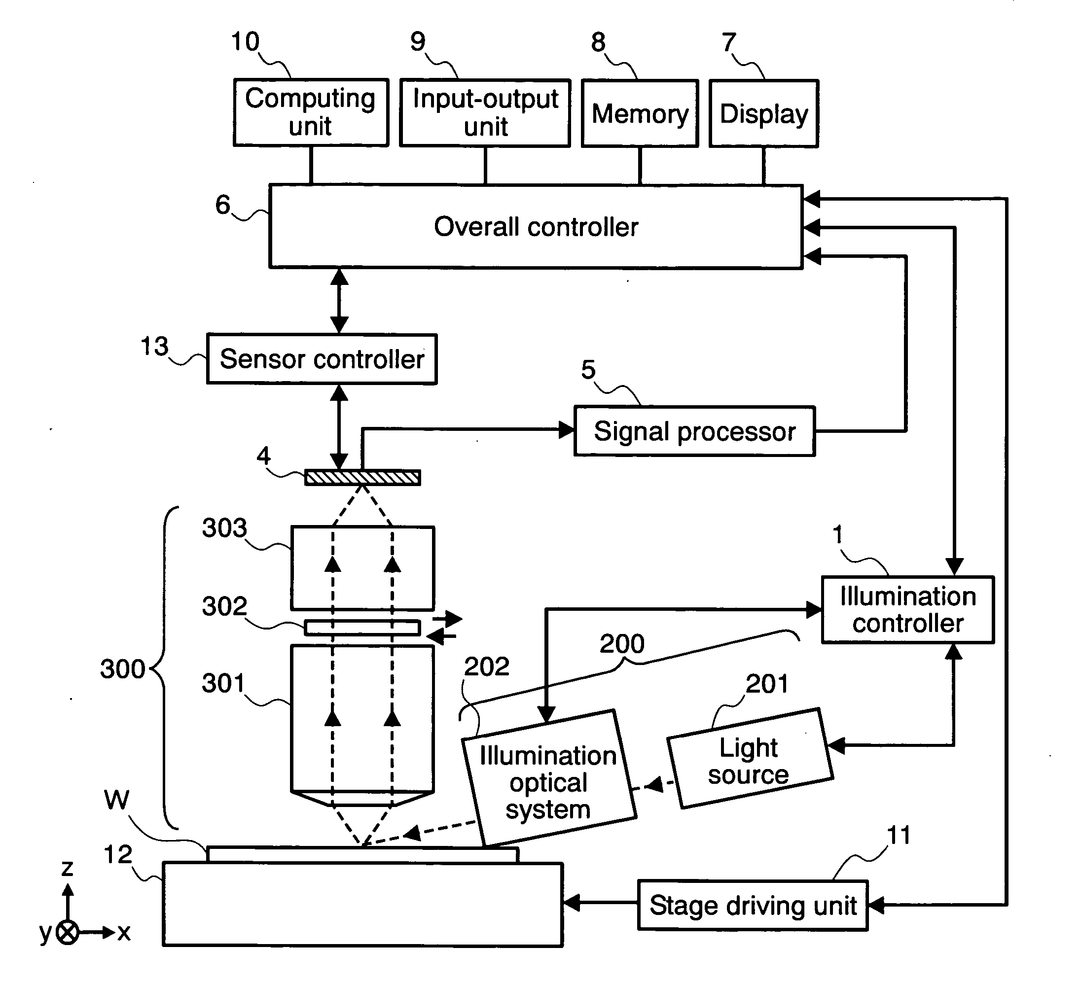
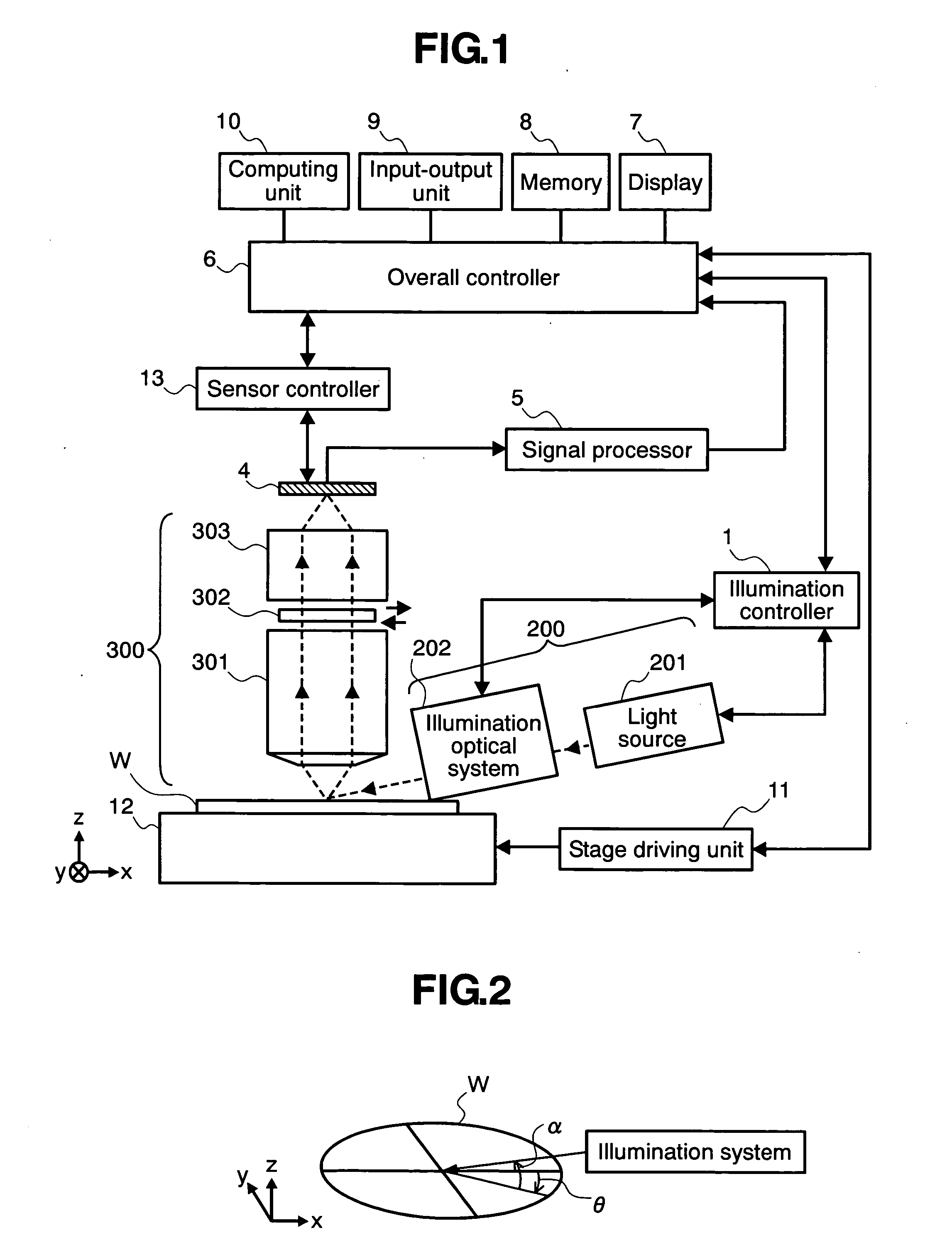
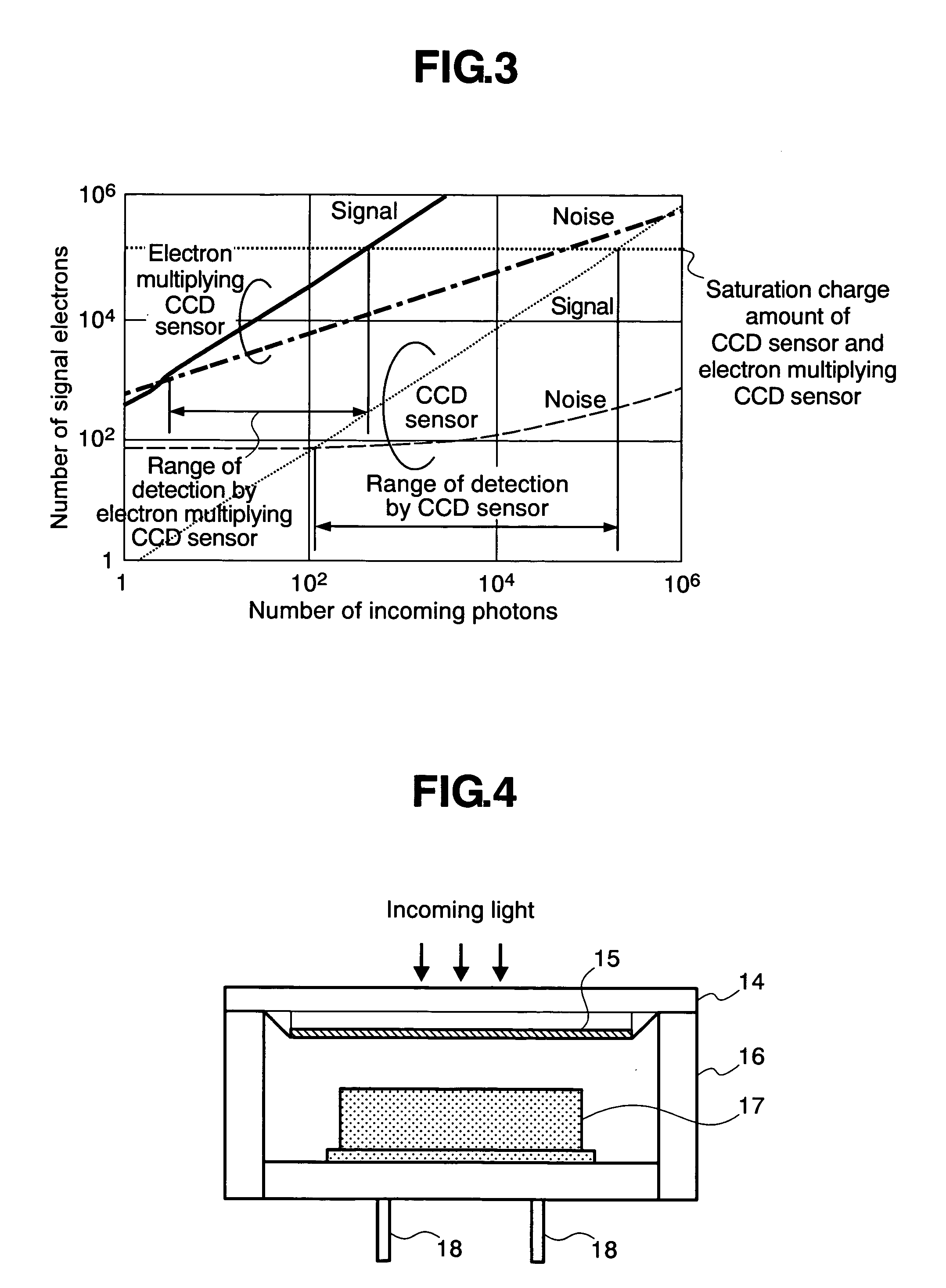
[0047]FIG. 1 shows an example of a device detecting foreign matters or defects on a semiconductor wafer. The device of FIG. 1 comprises an illumination controller 1, an illumination system 200, a subject (semiconductor wafer) W, a detection optical system 300, an electron multiplying CCD sensor 4, a signal processor 5, an overall controller 6, a display 7, a memory 8, an input-output unit 9, a computing unit 10, a stage driving unit 11, a stage 12, and a sensor controller 13. The illumination system 200 comprises a light source 201 and an illumination optical system 202. The detection optical system 300 comprises an objective lens 301, a spatial filter 302 removable by a moving means (not shown), and a tube lens 303.

[0048] Now, workings of the device will be described. First,...


PUM


Abstract

When using a CCD sensor as a photo-detector in a device for inspecting foreign matters and defects, it has a problem of causing electric noise while converting the signal charge, produced inside by photoelectric conversion, into voltage and reading it. Therefore, the weak detected signal obtained by detecting reflected and scattered light from small foreign matters and defects is buried in the electric noise, which has been an obstacle in detecting small foreign matters and defects. In order to solve the above problem, according to the present invention, an electron multiplying CCD sensor is used as a photo-detector. The electron multiplying CCD sensor is capable of enlarging signals brought about by inputted light relatively to the electric noise by multiplying the electrons produced through photoelectric conversion and reading them. Accordingly, compared to a conventional CCD sensor, it can detect weaker light and, therefore, smaller foreign matters and defects.

Description

BACKGROUND OF THE INVENTION [0001] 1. Field of the Invention [0002] The present invention relates to a method and device for detecting foreign matters and defects produced in the manufacturing processes of LSIs, liquid crystal substrates, etc. wherein patterns are formed on the substrates. [0003] 2. Description of the Related Art [0004] In the past, as disclosed in Japanese Patent Laid-open No. 62-89336, such a method for detecting foreign matters and defects on a semiconductor wafer is known that a laser beam is irradiated on the semiconductor wafer and scattered light from foreign matters is detected when there are such foreign matters on the semiconductor wafer and the foreign matters and defects are inspected by comparing the scattered light with an inspection result of a semiconductor wafer of the same kind inspected in advance. [0005] In the conventional device for inspecting foreign matters and defects, a CCD sensor has been used as a photo-detector. A CCD sensor is capable o...

Claims


Application Information

Patent Timeline
IPC IPC(8): G01N21/86G01N21/956H01L21/66H01L27/148H04N5/335H04N5/359H04N5/372
CPCG01N21/47G01N21/4788G01N21/94G01N21/9501G01N21/956
Inventor URANO, YUTANAKANO, HIROYUKIMAEDA, SHUNJIUTO, SACHIO
Owner HITACHI HIGH-TECH CORP
Why Eureka
Try Eureka