Buffer circuit
- Summary
- Abstract
- Description
- Claims
- Application Information
AI Technical Summary
Benefits of technology
Problems solved by technology
Method used
Image

Examples
first embodiment
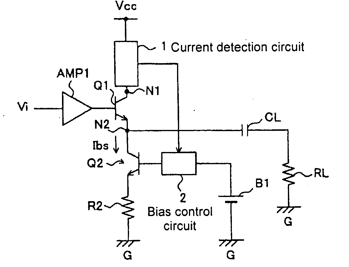
[0040]FIG. 1 is a diagram showing an example configuration of a buffer circuit pertaining to a first embodiment of the present invention.
[0041] The buffer circuit shown in FIG. 1 has npn transistors Q1 and Q2, current detection circuit 1, bias control circuit 2, resistor R2, and bias supply circuit B1.
[0042] Furthermore, npn transistor Q1 is an embodiment of the first transistor of the present invention.
[0043] The npn transistor Q2 is an embodiment of the second transistor of the present invention.
[0044] Current detection circuit 1 is an embodiment of the current detection circuit of the present invention.
[0045] Bias control circuit 2 is an embodiment of the bias control circuit of the present invention.
[0046] The npn transistor Q1 regulates a current flowing from node N1 to node N2 in accordance with a signal input to its base.
[0047] That is, npn transistor Q1 is connected to node N1 by its collector and to node N2 by its emitter, and an output signal of amplification circui...
second embodiment
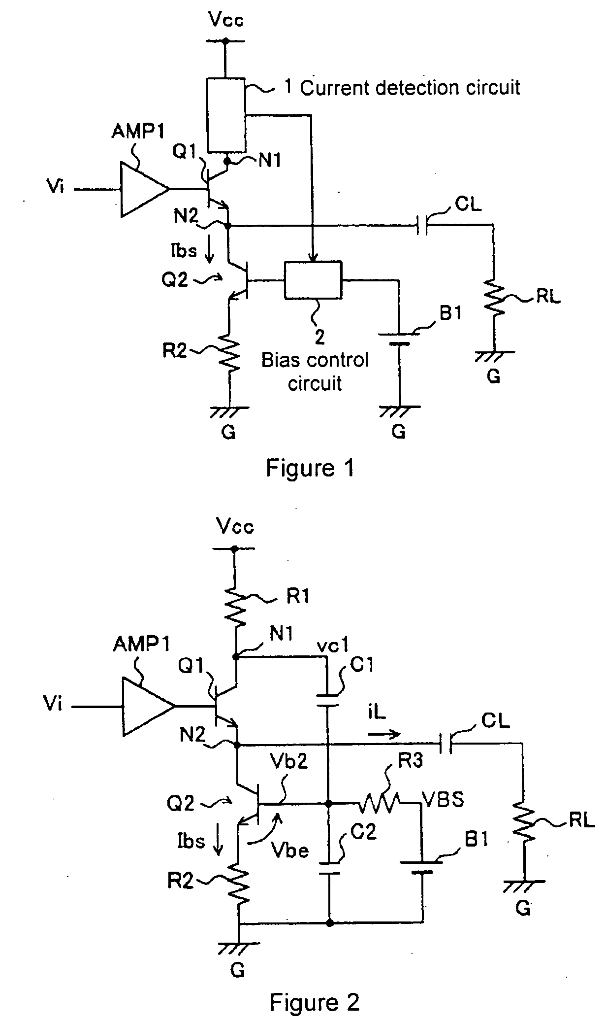
[0064] Next, a second embodiment of the present invention will be described.
[0065]FIG. 2 is a diagram showing an example configuration of a buffer circuit pertaining to a second embodiment of the present invention.
[0066] The buffer circuit shown in FIG. 2 has npn transistors Q1 and Q2, resistors R1 through R3, capacitors C1 and C2, and bias supply circuit B1.
[0067] Furthermore, resistor R1 is an embodiment of the impedance circuit of the present invention.
[0068] The circuit that contains resistor R3 and capacitors C1 and C2 is an embodiment of the bias control circuit of the present invention.
[0069] The series circuit comprising capacitors C1 and C2 is an embodiment of the capacitor series circuit of the present invention.
[0070] Resistor R3 is an embodiment of the resistor of the present invention.
[0071] Resistor R1 is connected between supply voltage line VCC and node N1.
[0072] Capacitor C1 is connected between the base of npn transistor Q2 and node N1.
[0073] Capacitor C2 ...
third embodiment
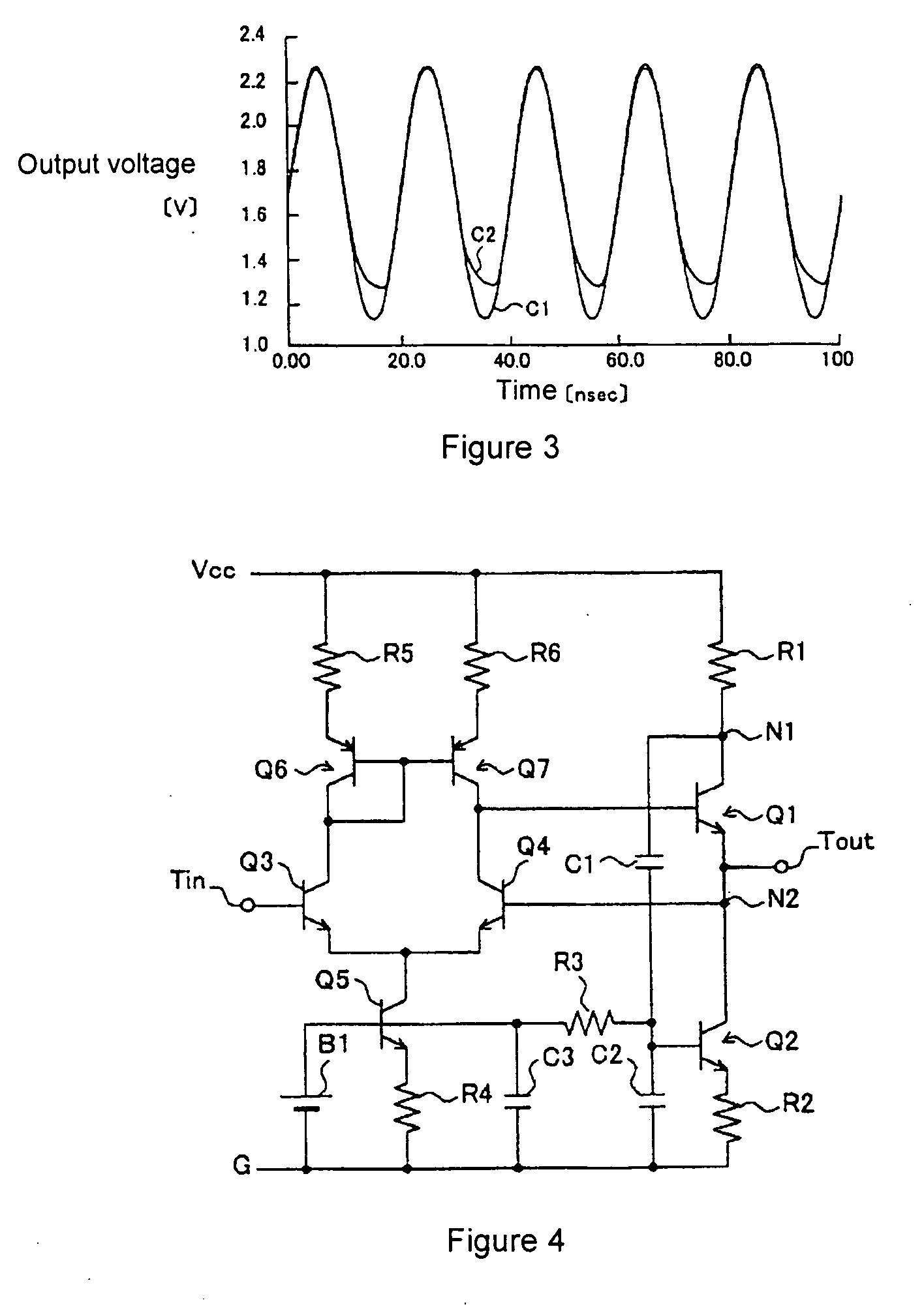
[0108] A third embodiment of the present invention will be described next.
[0109]FIG. 8 is a diagram showing an example configuration of a buffer circuit pertaining to a third embodiment of the present invention.
[0110] The buffer circuit shown in FIG. 8 has npn transistors Q1 and Q2, resistor R2, inductors L1 and L2, and bias supply circuit B1.
[0111] Furthermore, inductor L1 is an embodiment of the first inductor of the present invention.
[0112] Inductor L2 is an embodiment of the second inductor of the present invention.
[0113] Inductor L1 is inserted in a wiring line used to input a current from supply voltage line VCC to npn transistor Q1 via node N1.
[0114] Inductor L2 is joined magnetically with inductor L1, whereby it generates a voltage corresponding to the current flowing in inductor L1, superimposes it on the DC bias voltage of bias supply circuit B1, and supplies it to the base of npn transistor Q2. Inductor L2 is connected between the bias voltage output terminal of bia...
PUM
 Abstract
Description
Claims
Application Information
 - Generate Ideas
- Intellectual Property
- Life Sciences
- Materials
- Tech Scout
- Unparalleled Data Quality
- Higher Quality Content
- 60% Fewer Hallucinations
Browse by: Latest US Patents, China's latest patents, Technical Efficacy Thesaurus, Application Domain, Technology Topic, Popular Technical Reports.
© 2025 PatSnap. All rights reserved.Legal|Privacy policy|Modern Slavery Act Transparency Statement|Sitemap|About US| Contact US: help@patsnap.com