Planar filter, semiconductor device and radio unit

a filter and semiconductor technology, applied in the field of planar filters, can solve the problems of increasing the loss in the pass band and the area to be occupied by the filter, deteriorating the space efficiency of the ic chip, and increasing the dead space not available, so as to facilitate the fabrication of a semiconductor device, and reduce the cost of semiconductor devices

Active Publication Date: 2006-07-27
SHARP KK
View PDF4 Cites 24 Cited by
  • Summary
  • Abstract
  • Description
  • Claims
  • Application Information

AI Technical Summary

Benefits of technology

[0006] In consideration of these drawbacks, an object of the present invention is to provide a planar filter occupying a small area, suitable for integration on an IC chip, and having good wave filtration characteristics and good attenuation characteristics.

Problems solved by technology

It is to be noted that while a larger number of resonators can increase attenuation outside the band, it also increases loss in the pass band and the area to be occupied by the filter.
Particularly in the case where the planar filter is integrated on an IC chip for reducing a loss in a connection section between the planar filter and other high-frequency integrated circuits, the conventional resonator layout deteriorates space efficiency of the IC chip and increases dead space not available for other circuits, with the result that the size of the IC chip and the unit cost of the chip are increased.

Method used


Image

  • Planar filter, semiconductor device and radio unit
  • Planar filter, semiconductor device and radio unit
  • Planar filter, semiconductor device and radio unit

Examples


first embodiment

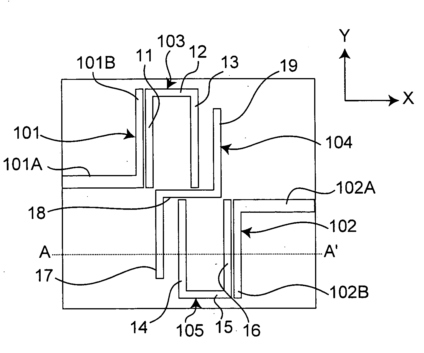
[0028]FIGS. 1A and 1B show a planar filter in the first embodiment of the present invention. FIG. 1A is a plan view, and FIG. 1B is a cross sectional view taken along line A-A′ in FIG. 1A. As shown in FIG. 1A, the planar filter in the first embodiment has a first input / output transmission line 101 serving as an input line, a second input / output transmission line 102 serving as an output line, a first U-shaped open transmission line resonator 103, a second U-shaped open transmission line resonator 105 and a crank-shaped open transmission line resonator 104, which are formed on a dielectric substrate 110. As shown in FIG. 1B, the dielectric substrate 110 has a grounding conductor 111 on its back face.

[0029] As shown in FIG. 1C, the first U-shaped open transmission line resonator 103 has bends so as to be in generally U shape, and is composed of three contiguous connected transmission lines 11, 12 and 13. The transmission lines 11 and 13 face each other in an almost parallel state, an...

second embodiment

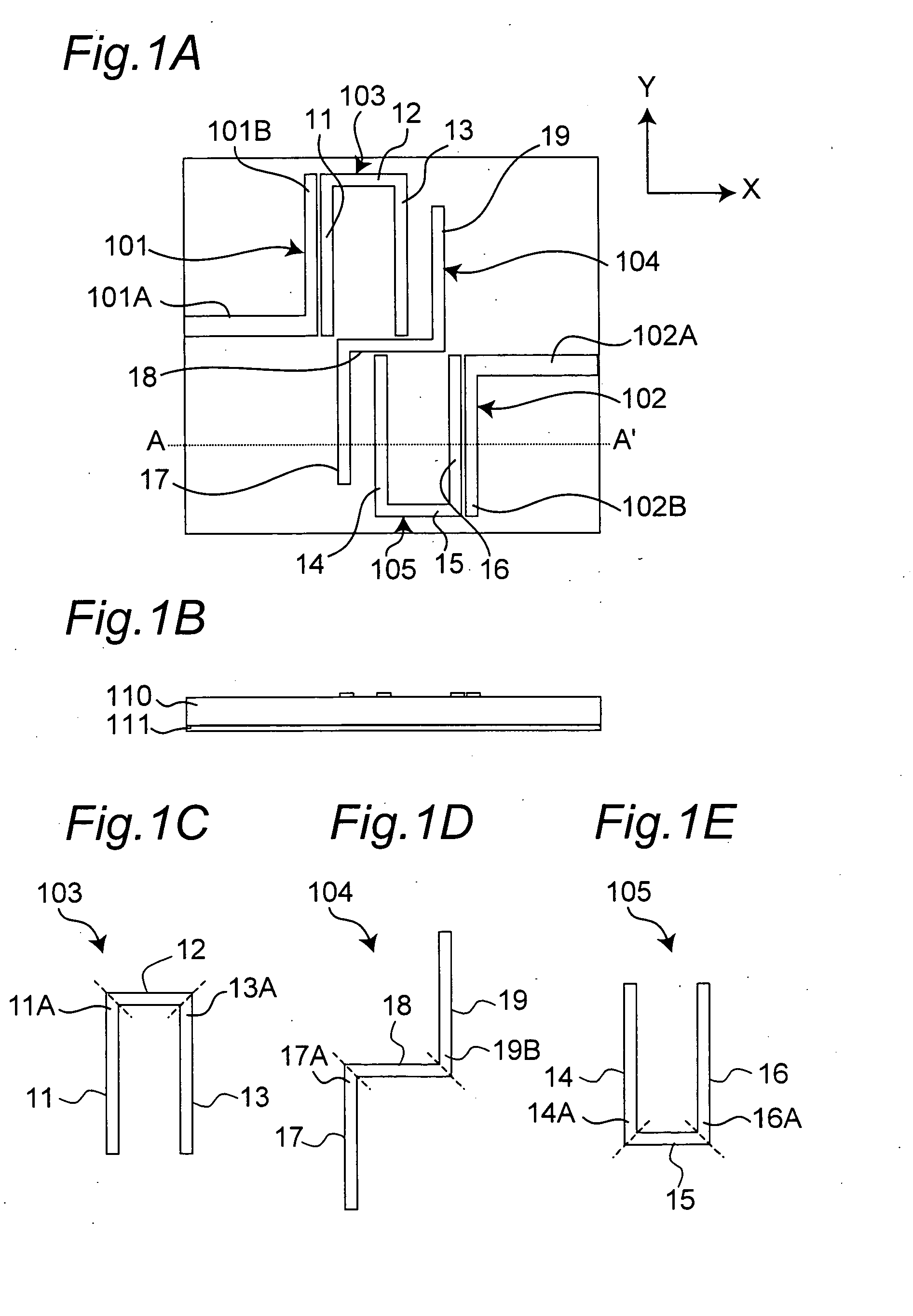
[0044]FIGS. 2A and 2B show a planar filter in the second embodiment of the present invention. FIG. 2A is a plan view, and FIG. 2B is a cross sectional view taken along line B-B′ in FIG. 2A.

[0045] The planar filter in the second embodiment has a first input / output transmission line 201 serving as an input line, a second input / output transmission line 202 serving as an output line, a first U-shaped open transmission line resonator 203, a second U-shaped open transmission line resonator 205 and a crank-shaped open transmission line resonator 204, which are formed on a semi-insulative gallium arsenide substrate 210 of a thickness of 70 μm. As shown in FIG. 2B, the semi-insulative gallium arsenide substrate 210 has a grounding conductor 211 on its back face.

[0046] As shown in FIG. 2C, the first U-shaped open transmission line resonator 203 has bends so as to be in generally U shape, and is composed of three contiguous connected transmission lines 21, 22 and 23. The transmission lines 2...

third embodiment

[0064] Next, FIGS. 4A and 4B show a planar filter-integrated even-harmonic mixer device that is a semiconductor device as a third embodiment of the present invention. FIG. 4A is a plan view and FIG. 4B is a cross sectional view taken along line C-C′ in FIG. 4A. The planar filter-integrated even-harmonic mixer device in the third embodiment is formed by integrating a planar filter 301 according to the second embodiment shown in FIG. 2 with an even-harmonic mixer 300 on a semiconductor substrate.

[0065] The even-harmonic mixer device in the third embodiment is an up-converter even-harmonic mixer device for converting an intermediate-frequency signal to a high-frequency signal. The mixer device receives an intermediate-frequency signal (having a frequency (fIF)) and a local oscillation signal (having a frequency (fLO)), and mixes the intermediate-frequency signal and the local oscillation signal to output a high-frequency signal (having a frequency (fRF)). The frequency (fIF), the freq...


PUM


Abstract

A planar filter has first and second U-shaped open transmission line resonators (103, 105) and a crank-shaped open transmission line resonator (104), so that it is possible to decrease an area to be virtually occupied by the filter on a dielectric substrate (110) and enhance the attenuation characteristic.

Description

BACKGROUND OF THE INVENTION [0001] The present invention relates to a planar filter suitable for use, for example, in microwave bands including millimeter wave bands, and more particularly to a planar filter preferable for use in high-frequency radio communication devices such as millimeter wave communication devices using a frequency of 30 GHz or more, as well as to a semiconductor device and a radio unit having the planar filter. [0002] Conventionally, there have been planar filters that use microstrip resonators. A design method thereof is described in, e.g., a literature “Basics and Applications of Microwave Circuits” by Yoshihiro Konishi, pages 369-373, published by Sogo Denshi Publishing, Aug. 20, 1990). [0003]FIGS. 6A and 6B show one example of conventional planar filters. FIG. 6A is a plan view and FIG. 6B is a cross sectional view taken along the line D-D′ in FIG. 6A. The planar filter is structured such that an input line 1, an output line 2, a resonator 3, a resonator 4 a...

Claims


Application Information

Patent Timeline
Patent Type & Authority Applications(United States)
IPC IPC(8): H01P1/203H01L21/822H01L27/04H01P1/205H01P7/08
CPCH01P1/20372H01P1/20381
Inventor YAMADA, ATSUSHI
Owner SHARP KK
Why Eureka
Try Eureka