Semiconductor device, display device and electronic apparatus

Inactive Publication Date: 2006-07-27
SEMICON ENERGY LAB CO LTD
View PDF19 Cites 44 Cited by
  • Summary
  • Abstract
  • Description
  • Claims
  • Application Information

AI Technical Summary

Benefits of technology

[0035] The invention can provide a display device in which even when characteristics of a transistor in an inverter in a pixel vary in each pixel, the effect can be reduced and a clear gradation can be displayed.
[0036] Furth

Problems solved by technology

Therefore, in a display device of a driving method for expressing a gradation in an analog time, even the same gradation display varies between pixels and clear display cannot be performed.
Further, there are problems in that the number of transistors or wires in a pixel is large, an aperture ratio decreases, and the like in conventional conf

Method used


Image

  • Semiconductor device, display device and electronic apparatus
  • Semiconductor device, display device and electronic apparatus
  • Semiconductor device, display device and electronic apparatus

Examples


embodiment mode 1

[0102] In this embodiment mode, described are a pixel configuration of a display device of the invention and a principal of operation thereof.

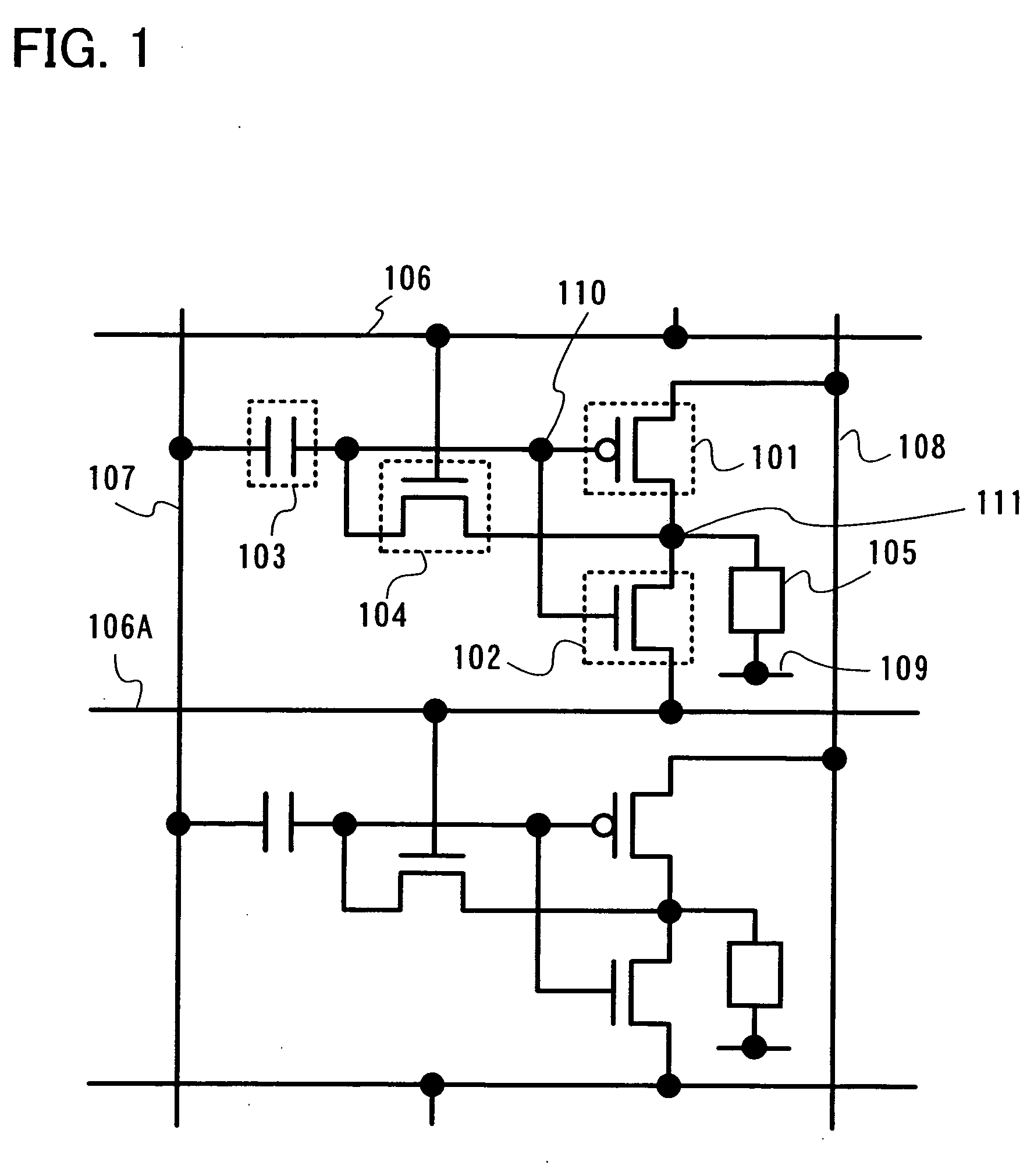
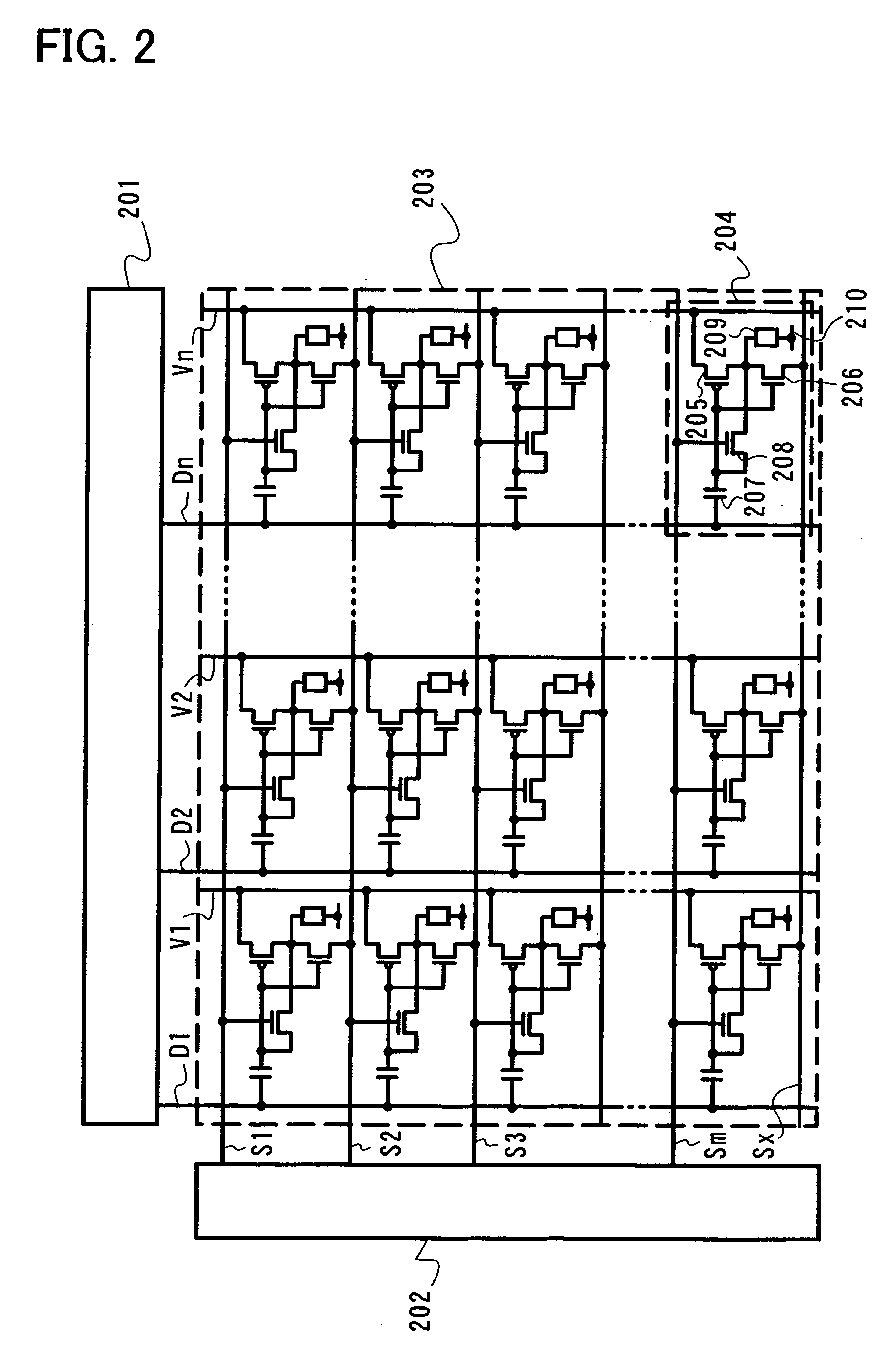
[0103] First, description is made in detail on a pixel configuration of a display device of the invention with reference to FIG. 1. Here, although only two pixels arranged in a column direction are shown, a plurality of pixels are arranged in matrix in a row direction and a column direction in a pixel portion of the display device in reality.

[0104] A pixel has a driving transistor (a second transistor) 101, a complementary transistor (a third transistor) 102, a capacitor 103, a switching transistor (a first transistor) 104, a light emitting element 105, a scan line (Select line) 106, a signal line (Data line) 107, and a power source line 108. Note that a P channel transistor is used for the driving transistor 101 while N channel transistors are used for the complementary transistor 102 and the switching transistor 104.

[0105] A first termina...

embodiment mode 2

[0200] In this embodiment mode, described is another pixel configuration different from the pixel configuration in Embodiment Mode 1. The pixel configuration shown in this embodiment mode is a configuration in which an analog signal potential supplied when an analog signal is written to a pixel and an analog potential for controlling lighting / non-lighting of a pixel are supplied to a pixel by different wires.

[0201] A pixel has a driving transistor (a second transistor) 601, a complementary transistor (a third transistor) 602, a capacitor 603, a switching transistor (a first transistor) 604, a light emitting element 605, a scan line (Select line) 606, a first switch 607, a second switch 608, a first signal line (Data line 1) 609, a second signal line (Data line 2) 610, and a power source line 611 as shown in FIG. 6. Note that a P channel transistor is used for the driving transistor 601 while N channel transistors are used for the complementary transistor 602 and the switching trans...

embodiment mode 3

[0255] In this embodiment mode, description is made on a pixel configuration and a display device of the invention in the case of using a potential control line capable of controlling a potential level by a signal instead of a power source line with a fixed potential, and a driving method thereof.

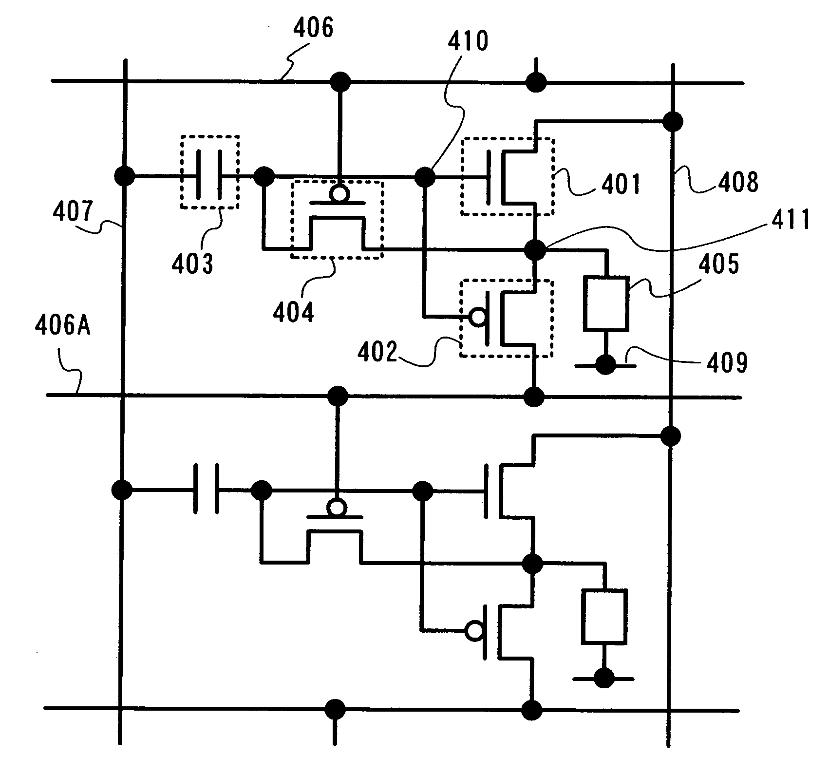
[0256]FIG. 48 shows a pixel configuration in the case of applying a potential supply line 4808 instead of the power source line 108 in the pixel configuration shown in FIG. 1.

[0257] A pixel has a driving transistor (a second transistor) 4801, a complementary transistor (a third transistor) 4802, a capacitor 4803, a switching transistor (a first transistor) 4804, a light emitting element 4805, a scan line (Select line) 4806, a signal line (Data line) 4807, and a potential supply line (Illumination line) 4808. Note that a P channel transistor is used for the driving transistor 4801 while N channel transistors are used for the complementary transistor 4802 and the switching transistor 4804. ...


PUM


Abstract

When a resistance load inverter is used to control lighting/non-lighting of a pixel, in accordance with characteristic variations of a transistor forming the resistance load inverter, variations occur in light emission of each pixel. As an inverter in a pixel, an N channel transistor and a P channel transistor are used to apply a CMOS inverter. Even when characteristics of the transistor forming the CMOS inverter vary and inverter transfer characteristics vary, there is little effect on controlling lighting/non-lighting of the pixel, therefore, light emission variations of each pixel can be eliminated. Further, a signal potential of a scan line is used as one power source of a potential of the inverter, therefore, an aperture ratio of the pixel can be increased.

Description

BACKGROUND OF THE INVENTION [0001] 1. Field of the Invention [0002] The present invention relates to a semiconductor device provided with a function to control a current supplied to a load by a transistor, particularly relates to a display device including a pixel formed of a current drive type light emitting element in which luminance varies according to a current, and a signal line driver circuit thereof. In addition, the invention relates to a driving method of the display device, and to an electronic apparatus having the display device in a display portion. [0003] 2. Description of the Related Art [0004] In recent years, a so-called self-luminous display device in which a pixel is formed of a light emitting element such as a light emitting diode (LED) has attracted attention. As a light emitting element used for such a self-luminous display device, an organic light emitting diode (an OLED), an organic EL element, an electroluminescence (EL) element, or the like have been attract...

Claims


Application Information

Patent Timeline
IPC IPC(8): G09G3/36H05B44/00
CPCG09G3/2014G09G3/3233G09G2300/0861H01L2251/568G09G2310/066G09G2320/0247G09G2300/0866H10K71/861
Inventor KIMURA, HAJIME
Owner SEMICON ENERGY LAB CO LTD
Why Eureka
Try Eureka