Method for manufacturing semiconductor substrate, semiconductor device and electronic device

a semiconductor substrate and semiconductor technology, applied in semiconductor devices, electrical devices, transistors, etc., can solve the problems of low heat resistance of glass substrates, temperature limitation to 700°, and glass substrates cannot be heated at a temperature exceeding 700°, so as to improve the planarity, improve the quality of single crystal semiconductor layers, and improve the effect of planarity

Inactive Publication Date: 2009-05-07
SEMICON ENERGY LAB CO LTD
View PDF38 Cites 41 Cited by
  • Summary
  • Abstract
  • Description
  • Claims
  • Application Information

AI Technical Summary

Benefits of technology

[0021]As one of the advantageous effects of the method for manufacturing a semiconductor substrate according to the present invention, the surface and a certain region in the depth direction of the single crystal semiconductor layer can be melted by laser irradiation from the single crystal semiconductor layer side. In this manner, the surface of the single crystal semiconductor layer, which is an irradiation surface, can have drastically improved planarity due to surface tension effect.
[0022]As one of the advantageous effects of the method for manufacturing a semiconductor substrate according to the present invention, the single crystal semiconductor layer is irradiated with a laser beam and heated so that lattice defects in the single crystal semiconductor layer generated in forming a damaged layer in the single crystal semiconductor substrate can be reduced, and thus a more excellent single crystal semiconductor layer can be obtained. In the laser-irradiated region of the single crystal semiconductor layer, the surface and a certain region in the thickness direction of the single crystal semiconductor layer are melted, and recrystallization progress in accordance with plane orientation of the single crystal semiconductor layer which is left without being melted, and thus a single crystal semiconductor layer having excellent characteristics can be obtained.
[0023]In the above References 1 to 5, mechanical polishing is performed as a main process for planarization; therefore, the above References 1 to 5 differ...

Problems solved by technology

However, the strain point of the glass substrate is equal to or lower than 700° C., and thus the glass substrate has low heat resistance.
Therefore, the glass substrate cannot be heated at a temperature which exceeds an allowable temperature limit of the glass substrate, and the process temperature is limited to 700° C. or lower.
That is, there is a limitation on a process temperature in a step of removing a crystal defect at a separation plane and a step of planarizing a surface.
In a conventional manner, a crystal defect of a semiconductor layer attached to a silicon wafer can be removed by heating at a temperature of 1000° C. or higher; however, such a high temperature process cannot be utilized for removal of a crystal defect of a semiconductor layer that is attached to a glass substrate having a strain point of 700° C...

Method used


Image

  • Method for manufacturing semiconductor substrate, semiconductor device and electronic device
  • Method for manufacturing semiconductor substrate, semiconductor device and electronic device
  • Method for manufacturing semiconductor substrate, semiconductor device and electronic device

Examples


embodiment mode 1

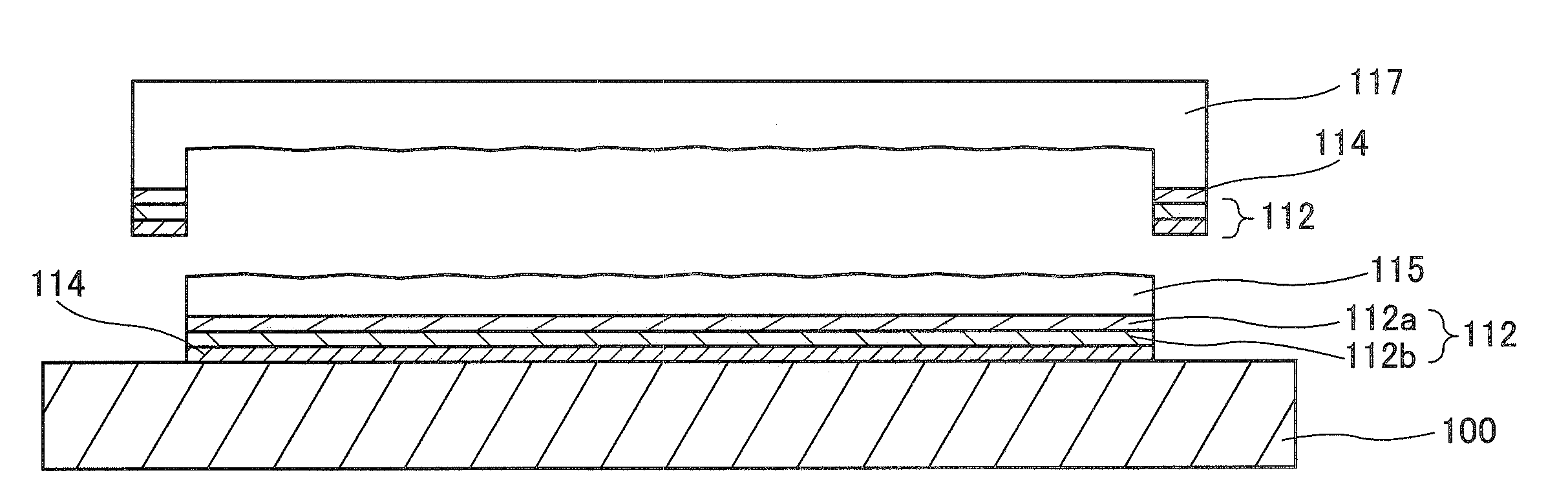
[0077]FIG. 1 is a perspective view of an example of a semiconductor substrate structure. In a semiconductor substrate 10, a single crystal semiconductor layer 116 is attached to a supporting substrate 100 with a buffer layer 101 interposed therebetween. The semiconductor substrate 10 is a substrate having a so-called SOI structure and has a single crystal semiconductor layer over an insulating layer.

[0078]The buffer layer 101 has a single layer structure or a multilayer structure in which two or more films are stacked. In this embodiment mode, the buffer layer 101 has a three-layer structure in which a bonding layer 114, an insulating film 112b and an insulating film 112 are stacked over the supporting substrate 100. In addition, the insulating film 112a is an insulating film serving as a barrier layer. The barrier layer can prevent an impurity (typically, sodium) of an alkali metal or an alkaline earth metal which may reduce reliability of a semiconductor device from entering the s...

embodiment mode 2

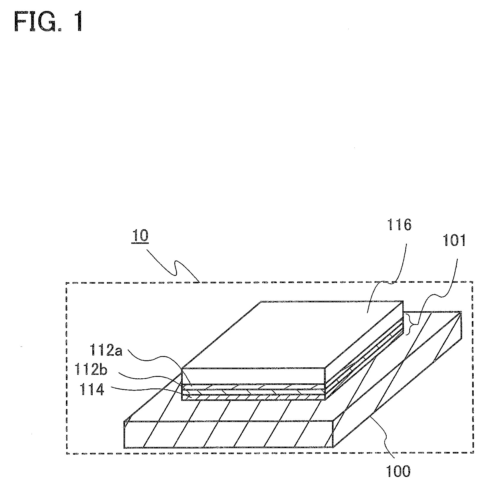
[0229]A single crystal semiconductor substrate 117 from which a single crystal semiconductor layer 115 has been separated can be reused as the single crystal semiconductor substrate 110 by being subjected to reprocessing treatment. In this embodiment mode, the reprocessing treatment is described.

[0230]As shown in FIG. 4A, a portion which is not attached to the supporting substrate 100 is left remaining at the periphery of the single crystal semiconductor substrate 117. Portions of the insulating film 112b, the insulating film 112a, and the bonding layer 114 which are not attached to the supporting substrate 100 remain in this portion.

[0231]First, etching treatment is performed to remove the insulating film 112a, the insulating film 112a, and the bonding layer 114. For example, when these films are formed from silicon oxide, silicon oxynitride, or silicon nitride oxide, the insulating film 112b, the insulating film 112a, and the bonding layer 114 can be removed by wet etching treatme...

embodiment mode 3

[0236]As an example of a manufacturing method of a semiconductor device using the semiconductor substrate 10, a manufacturing method of transistors will be described in Embodiment Mode 3, with reference to cross-sectional views of FIGS. 16A to 16D, FIGS. 17A to 17C, and FIGS. 18A and 18B. By combining a plurality of transistors, a variety of types of semiconductor devices are manufactured. In this embodiment mode, an n-channel transistor and a p-channel transistor can be manufactured at the same time.

[0237]As illustrated in FIG. 16A, a single crystal semiconductor layer over the supporting substrate 100 is processed (patterned) into a desired shape by etching, so that a semiconductor film 603 and a semiconductor film 604 are formed. A p-channel transistor is formed using the semiconductor film 603, and an n-channel transistor is formed using the semiconductor film 604.

[0238]To control threshold voltages, a p-type impurity element such as boron, aluminum, or gallium or an n-type impu...


PUM


Abstract

A semiconductor substrate including a single crystal semiconductor layer with a buffer layer interposed therebetween is manufactured. A semiconductor substrate is doped with hydrogen to form a damaged layer containing a large amount of hydrogen. After the single crystal semiconductor substrate and a supporting substrate are bonded, the semiconductor substrate is heated so that the single crystal semiconductor substrate is separated along a separation plane. The single crystal semiconductor layer is irradiated with a laser beam from the single crystal semiconductor layer side to melt a region in the depth direction from the surface of the laser-irradiated region of the single crystal semiconductor layer. Recrystallization progresses based on the plane orientation of the single crystal semiconductor layer which is solid without being melted; therefore, crystallinity of the single crystal semiconductor layer is recovered and the surface of the single crystal semiconductor layer is planarized.

Description

BACKGROUND OF THE INVENTION[0001]1. Field of the Invention[0002]The present invention relates to a method for manufacturing a semiconductor substrate over which a single crystal semiconductor layer is fixed with a buffer layer interposed therebetween, a semiconductor device manufactured by the method, and an electronic device including the semiconductor device.[0003]2. Description of the Related Art[0004]In recent years, integrated circuits using an SOI (silicon on insulator) substrate, instead of using a bulk silicon wafer, have been developed. By utilizing characteristics of a thin single crystal silicon layer formed over an insulating layer, semiconductor layers of transistors formed in the integrated circuit can be electrically separated from each other completely. Further, since the fully depleted transistors can be formed, a semiconductor integrated circuit with high added value such as high integration, high speed driving, and low power consumption can be realized.[0005]As an...

Claims


Application Information

Patent Timeline
IPC IPC(8): H01L21/762H01L29/06H01L21/02H01L21/265H01L21/268H01L21/322H01L21/336H01L27/12H01L29/786
CPCH01L21/02532H01L21/02686H01L29/66772H01L27/1214H01L27/1266H01L21/76254H01L27/1218H01L27/1285H01L21/20
Inventor SHIMOMURA, AKIHISAISAKA, FUMITONAGANO, YOJIMOMO, JUNPEI
Owner SEMICON ENERGY LAB CO LTD
Why Eureka
Try Eureka