Semiconductor device and method of fabricating the same

a technology of semiconductor devices and semiconductors, applied in the direction of semiconductor devices, basic electric elements, electrical equipment, etc., can solve the problems of increasing the leakage current flowing through the control gate electrode, low density of high-dielectric-constant films,

Inactive Publication Date: 2006-07-27
KK TOSHIBA
View PDF2 Cites 317 Cited by
  • Summary
  • Abstract
  • Description
  • Claims
  • Application Information

AI Technical Summary

Problems solved by technology

Unfortunately, the density of a high-dielectric-constant film is low.
This increases a leakage current flowing through the control gate electrode.

Method used


Image

  • Semiconductor device and method of fabricating the same
  • Semiconductor device and method of fabricating the same
  • Semiconductor device and method of fabricating the same

Examples


first embodiment

(1) First Embodiment

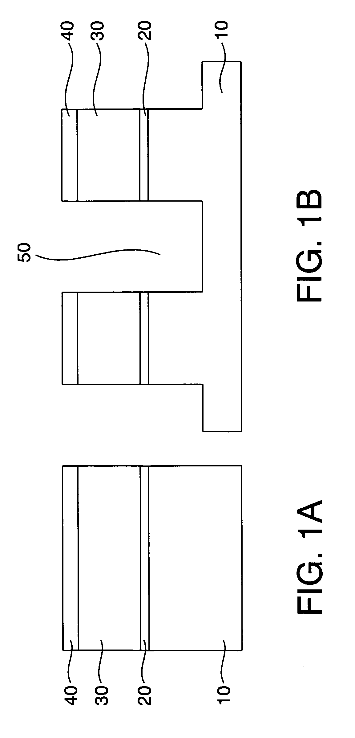
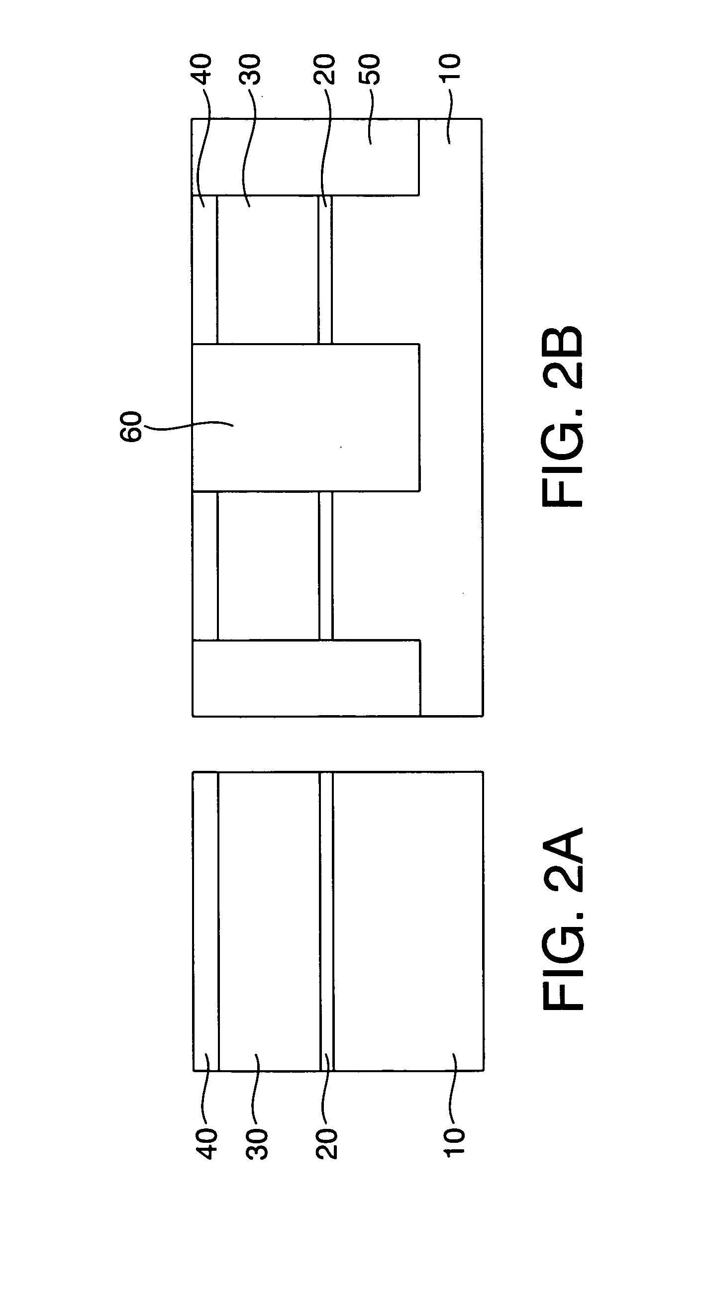
[0043]FIGS. 1A to 6B show a method of fabricating a memory cell transistor of a NAND flash memory according to the first embodiment of the present invention. Of FIGS. 1A to 5B, each of FIGS. 1A, 2A, 3A, 4A, and 5A is a longitudinal sectional view, cut along a bit line, of elements in a predetermined step, and each of FIGS. 1B, 2B, 3B, 4B, and 5B is a longitudinal sectional view, cut along a word line, of elements in a predetermined step.

[0044] First, as shown in FIGS. 1A and 1B, a silicon oxynitride (SiON) film 20 about 10 nm thick serving as a tunnel insulating film is formed by thermal oxidation and thermal nitriding on a semiconductor substrate 10 into which a predetermined impurity is doped. After that, a phosphorous (P)-doped polysilicon layer 30 serving as a floating gate electrode is deposited by CVD (Chemical Vapor Deposition), and a mask material 40 is formed by coating. Note that any of various impurities such as arsenic (As) may also be doped, in plac...

second embodiment

(2) Second Embodiment

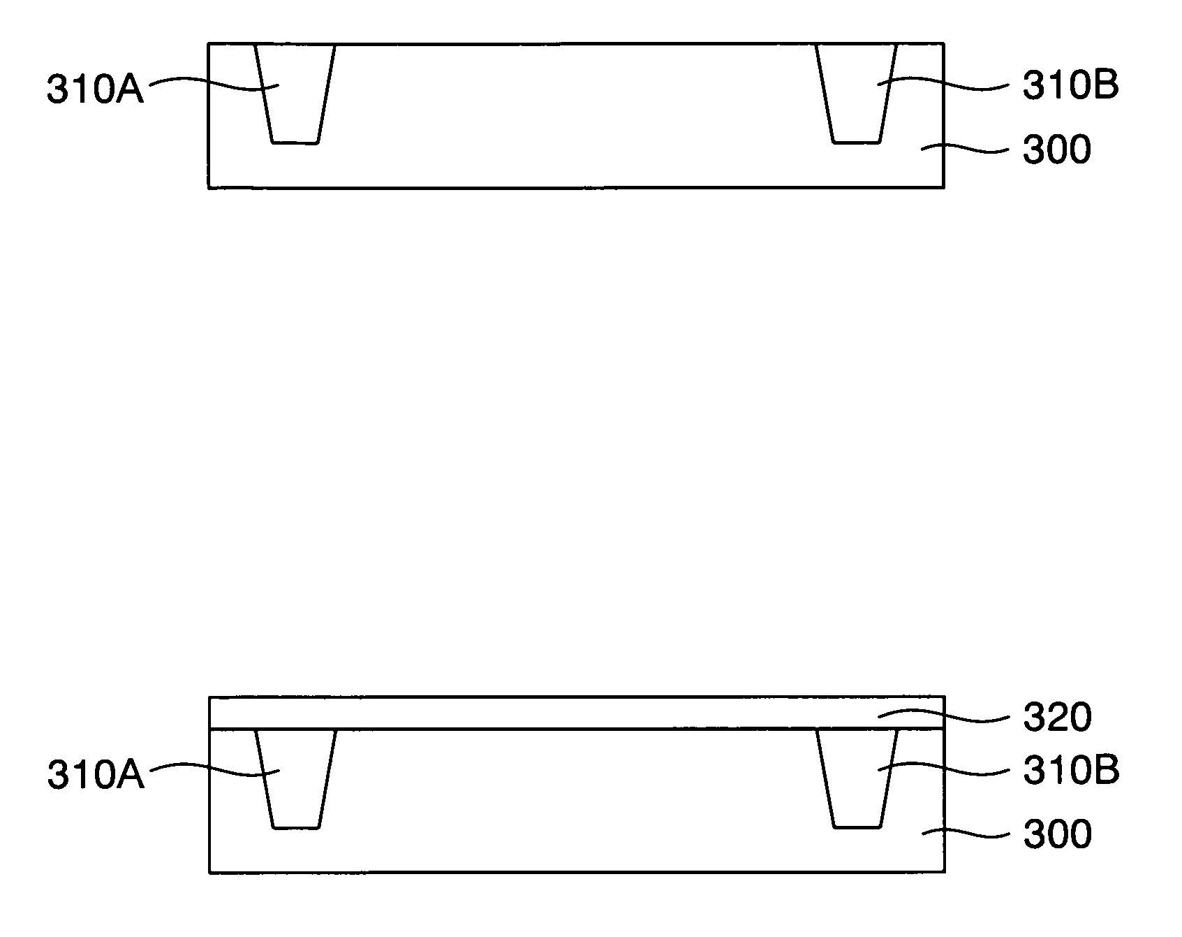
[0092] FIGS. 14 to 18 show a method of fabricating a MOSFET according to the second embodiment of the present invention. First, as shown in FIG. 14, element isolation insulating films 310A and 310B are formed on a semiconductor substrate 300, and a natural oxide film formed on the semiconductor substrate 300 is removed by cleaning using dilute hydrofluoric acid.

[0093] As shown in FIG. 15, the semiconductor substrate 300 is loaded into a batch type deposition / modification apparatus 65 shown in FIG. 7 which is a processing chamber having a single processing vessel and is called a furnace. In the deposition / modification apparatus 65, a hafnia (HfO2) film 320 serving as a gate insulting film is deposited on the surface of the semiconductor substrate 300 at a temperature of 400° C. Note that the deposition / modification apparatus 65 has an exhausting mechanism and gas supply source (neither is shown), and can form a desired ambient by using them.

[0094] In this embod...


PUM


Abstract

According to the present invention, there is provided a semiconductor device fabrication method comprising: forming a first insulating film on a semiconductor substrate; forming a first conductive layer on the first insulating film; forming a second insulating film on the first conductive layer in a first processing chamber isolated from an outside; performing a modification process on the second insulating film in the first processing chamber, and unloading the semiconductor substrate from the first processing chamber to the outside; annealing the second insulating film in a second processing chamber; and forming a second conductive layer on the second insulating film.

Description

CROSS REFERENCE TO RELATED APPLICATION [0001] This application is based upon and claims benefit of priority under 35 USC §119 from the Japanese Patent Application No. 2005-15415, filed on Jan. 24, 2005, the entire contents of which are incorporated herein by reference. BACKGROUND OF THE INVENTION [0002] The present invention relates to a semiconductor device and a method of fabricating the same. [0003] Conventionally, a NAND flash memory has been developed as a nonvolatile semiconductor memory. A memory cell transistor of this NAND flash memory has a structure in which a floating gate electrode formed on a semiconductor substrate via a tunnel insulating film and a control gate electrode formed on this floating gate electrode via an inter-electrode insulating film are stacked. [0004] Recently, to decrease the cell size, a method of using an alumina (Al2O3) film, instead of the conventional ONO film (a stacked film in which a silicon oxide film, silicon nitride film, and silicon oxide...

Claims


Application Information

Patent Timeline
Patent Type & Authority Applications(United States)
IPC IPC(8): H01L21/8238H01L21/336
CPCH01L21/324H01L27/115H01L27/11521H01L27/11524H01L21/3247H01L29/40114H10B41/35H10B69/00H10B41/30
Inventor KAMIOKA, ISAOOZAWA, YOSHIO
Owner KK TOSHIBA
Why Eureka
Try Eureka