

Light emitting device and electronic device
- Summary
- Abstract
- Description
- Claims
- Application Information
AI Technical Summary
Benefits of technology
Problems solved by technology
Method used
Image

Examples
embodiment mode 1
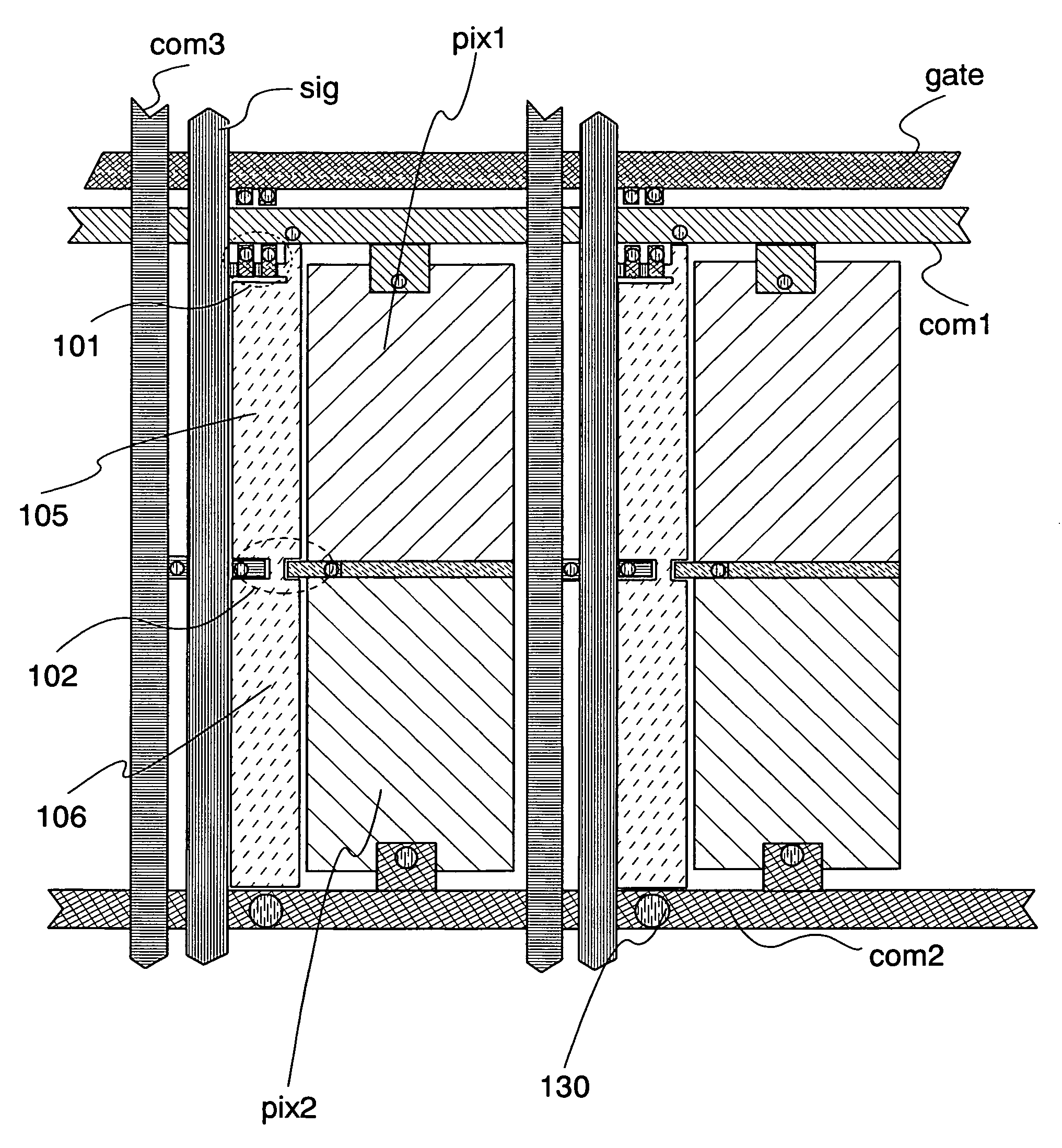
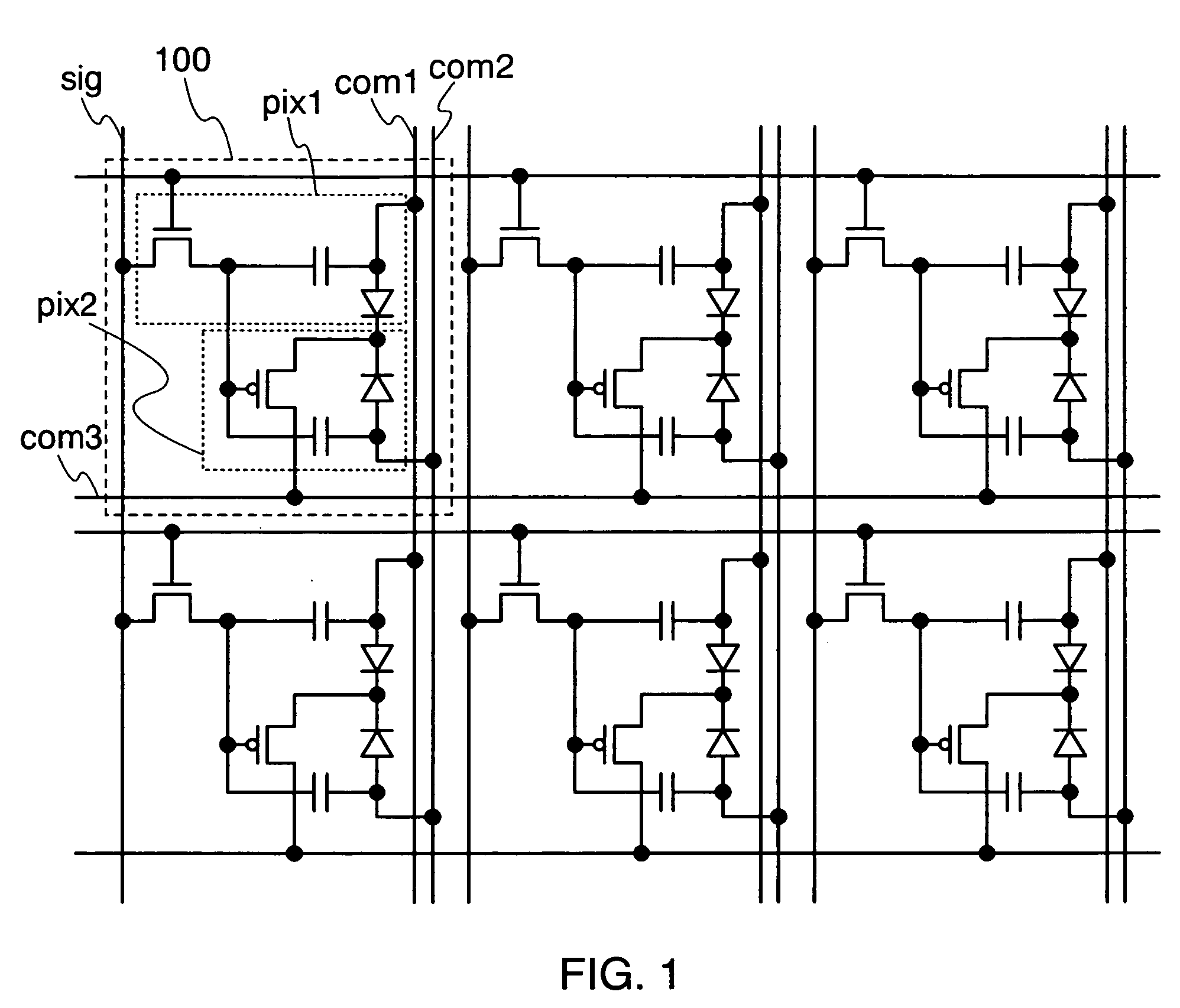
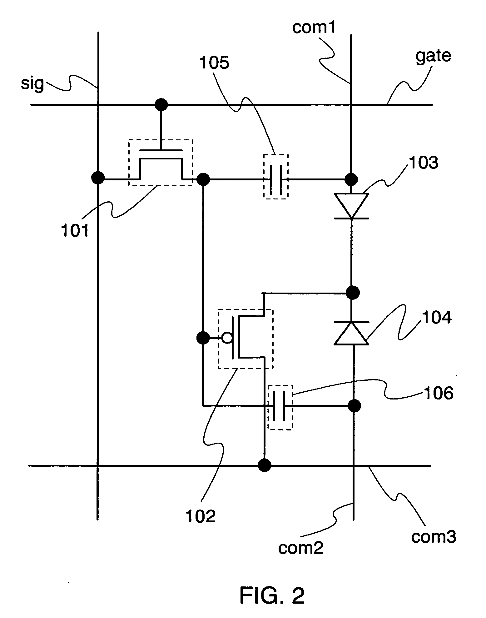
[0076]FIG. 1 shows a circuit diagram in which pixel portions of this embodiment mode are arranged in matrix. FIG. 2 shows an enlarged circuit configuration of a circuit in the pixel portion of this embodiment mode. A region 100 shown in FIG. 1 includes a first pixel pix1 and a second pixel pix2. Further, each of the region 100 shown in FIG. 1 and the enlarged region 100 shown in FIG. 2 includes a scan line gate, a data line sig, a first power source line com1, a second power source line com2, and a third power source line com3.
[0077] It is to be noted in the invention that a pixel portion refers to a region provided at each intersection of a plurality of scan lines and a plurality of data lines. In this embodiment mode, the region 100 corresponds to a pixel portion.
[0078] In FIG. 2, the pixel portion includes a selecting transistor 101, a driving transistor 102, a first light emitting element 103, a second light emitting element 104, a first capacitor 105, and a second capacitor 1...
embodiment mode 2
[0126] In Embodiment Mode 1, the description is made on the circuit diagram of the light emitting device where a common driving transistor is driven for both the first light emitting element and the second light emitting element usually, thereby a reverse bias voltage is applied to the second light emitting element while the first light emitting element emits light. In this embodiment mode, a specific configuration where a driving transistor is provided for each of the first light emitting element and the second light emitting element is described below.
[0127]FIG. 9 shows a circuit diagram where pixels of this embodiment mode are arranged in matrix. FIG. 10 shows an enlarged circuit configuration of a pixel portion of this embodiment mode. The region 100 as a pixel portion shown in FIG. 9, which is the pixel portion, includes the first pixel pix1 and the second pixel pix2. Further, each of the regions 100 shown in FIG. 9 and the enlarged region 100 shown in FIG. 10 includes a scan ...
embodiment mode 3
[0151] In the aforementioned embodiment mode, an erasing transistor may be provided for erasing the electrical potentials held in the first capacitor and the second capacitor. Specific configurations thereof are described below.
[0152]FIG. 13 shows a circuit diagram where pixel portions of this embodiment mode are arranged in matrix. FIG. 14A shows an enlarged circuit configuration of the pixel portion of this embodiment mode. The region 100 shown in FIG. 13 includes the first pixel pix1 and the second pixel pix2. Further, each of the region 100 shown in FIG. 13 and the enlarged region 100 shown in FIG. 14A includes a scan line gate1, an erase line gate2, a data line sig, a first power source line com1, and a second power source line com2.
[0153] In FIG. 14A, the pixel portion includes the selecting transistor 101, the first driving transistor 1001, the second driving transistor 1002, an erasing transistor 1401, the first light emitting element 103, the second light emitting element...
PUM
 Abstract
Description
Claims
Application Information