Method and apparatus for packaging an electronic chip

a technology of electronic chips and packaging, applied in electrical apparatus, semiconductor devices, semiconductor/solid-state device details, etc., can solve the problems of poor thermal performance, high input/output conductance, and usually higher cost, and achieve accurate positioning and removal of heat from array packages

Inactive Publication Date: 2006-08-03
TEXAS INSTR INC
View PDF8 Cites 75 Cited by
  • Summary
  • Abstract
  • Description
  • Claims
  • Application Information

AI Technical Summary

Benefits of technology

[0010] It will also be appreciated, that a rectangular (including square) electronic chip may be located such that two or more rows of terminal pads may exist on one or more of the four sides of a rectangular shaped electronic chip. Further, when the electronic chip is a flip chip, and the connection points are solder bumps, selected ones of the terminal pads may define divots for accurately locating the electronic chip on the grid frame. In addition, to aid in heat removal of a package, a flip chip may also include a heat conductive layer on its top surface, which includes heat conductive legs extending from the heat conductive layer to selected perimeter pads of the terminal pads so as to help remove heat from the array package.

Problems solved by technology

However, as will be appreciated, almost every new solution has its own problems and disadvantages.
For example, the disadvantages of the BGA packaging compared to lead frame based packages include: higher input / output conductance, poor thermal performance, and usually higher cost.

Method used


Image

  • Method and apparatus for packaging an electronic chip
  • Method and apparatus for packaging an electronic chip
  • Method and apparatus for packaging an electronic chip

Examples


Embodiment Construction

[0025] The making and using of the presently preferred embodiments are discussed in detail below. It should be appreciated, however, that the present invention provides many applicable inventive concepts that can be embodied in a wide variety of specific contexts. The specific embodiments discussed are merely illustrative of specific ways to make and use the invention, and do not limit the scope of the invention.

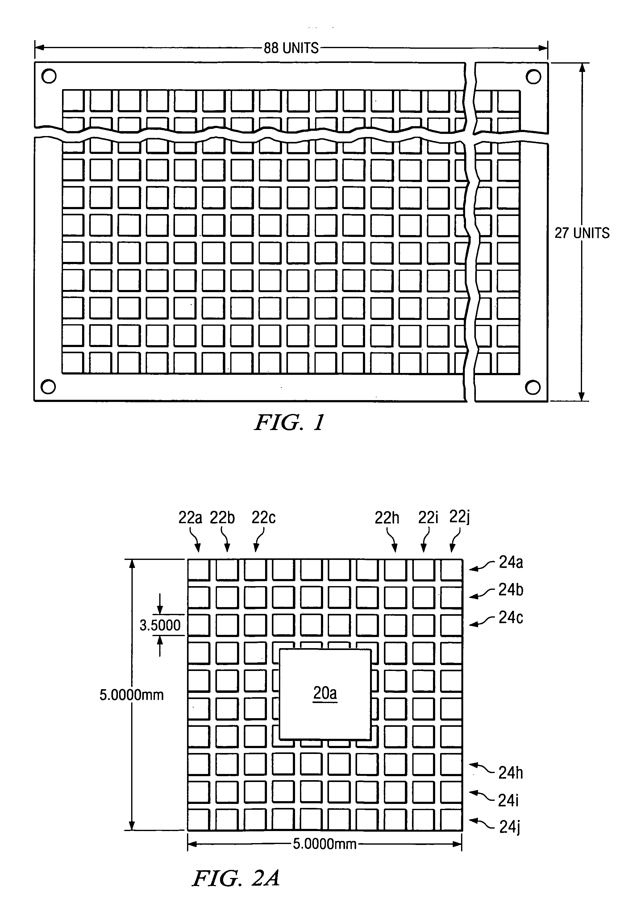
[0026] Referring now to FIG. 1, there is shown as an example a grid frame strip design according to the teachings of the present invention. As shown, the grid frame may be either a stamped or etched sheet of conductive material, such as copper or a copper alloy, and may also be pre-plated to allow for effective wire bonding. As will be discussed below, a grid may be etched in the grid frame substrate or alternately, several passes with a thin saw can produce a combination of saw kerfs that can be used to form the grids. In any event, and as will be discussed in detail herei...


PUM


Abstract

An electronic packaging combines features of a MAP (molded array package) and a lead frame package. The package includes an electrically conductive substrate somewhat like a lead frame package but defines a grid of conductive pads rather than a multiplicity of leads as is common with a lead frame package. An electronic chip is attached to the top surface of the lead frame, and the output terminals of the electronic chip are individually electrically connected to selected connecting pads of the lead frame grid array. Both flip chips and wire bond chips may be connected to the grid array. The channels defining the grid of connecting pads extend part way through the conductive substrate and increase in width from the top surface of the lead frame to the bottom of the channel such that the molding compound is locked in place when it cures and hardens. The grid pads are then singulated by sawing or etching channels from the bottom surface of the lead frame substrate that correspond to the channels defining the connecting pads on the top surface.

Description

TECHNICAL FIELD [0001] The present invention relates generally to integrated circuit chip package technology and more particular to a package that advantageously combines lead frame technology and MAP (mold array package) technology. BACKGROUND [0002] Integrated circuit dies are conventionally enclosed in plastic packages that provide protection from hostile environments and enable electrical interconnection between the integrated circuit die and an underlying substrate such as a printed circuit board. The elements of such a package include a metal lead frame, an integrated circuit die, bonding material to attach the integrated circuit die to the lead frame, bond wires, which electrically connect the pads on the integrated circuit die to individual leads of the lead frame, and a hard plastic encapsulant material which covers the components and forms the exterior of the package. [0003] The lead frame is the central supporting structure of the package and a portion of the lead frame i...

Claims


Application Information

Patent Timeline
Patent Type & Authority Applications(United States)
IPC IPC(8): H01L23/495
CPCH01L21/4832H01L2924/19105H01L23/4952H01L23/49575H01L25/0655H01L2224/16H01L2224/48091H01L2224/48247H01L2924/01078H01L2924/19041H01L23/4951H01L2224/73253H01L24/48H01L2924/01087H01L2224/16245H01L2924/00014H01L2924/14H01L2924/181H01L2224/97H01L24/49H01L2224/49175H01L2924/00011H01L2924/00H01L2224/0401H01L2924/00012H01L2224/45099H01L2224/45015H01L2924/207
Inventor GERBER, MARK ALLENKUDOH, TAKAHIKOMASAMOTO, MUTSUMIHERNANDEZ-LUNA, ALEJANDRO
Owner TEXAS INSTR INC
Why Eureka
Try Eureka