Using a polaron interaction zone as an interface to integrate a plasmon layer and a semiconductor detector

a technology of interaction zone and interface, applied in the field of integrated plasmon detectors, can solve the problems of limited approach, difficult detection of lithium, and inability to fully integrate lithium, and achieve the effect of reducing the energy of electrons emitted

Inactive Publication Date: 2006-08-03
CALIFORNIA INST OF TECH
View PDF6 Cites 4 Cited by
  • Summary
  • Abstract
  • Description
  • Claims
  • Application Information

AI Technical Summary

Benefits of technology

[0016] In another embodiment described herein, a plasmon detector comprises means for generating a plasmon on a metal; means for reducing the energy of electrons emitted by decay of the plasmon; and means for counting the reduced energy electrons.

Problems solved by technology

This imbalance of charge leads the jellium to disintegrate by the expulsion of both electrons such that total momentum is conserved.
However, if it does not pass through an adaptor layer to cool down quickly, the remaining heat will make detecting it functionally difficult.
This approach is limited by the fact that the decay photons have to travel a relatively long path from the surface to the detector, a path over which they undergo angular spreading misalignment, and environment influences.
Thus, collection and detection of decay photons as a means of studying plasmon effects can be difficult and prone to inaccuracies.

Method used


Image

  • Using a polaron interaction zone as an interface to integrate a plasmon layer and a semiconductor detector
  • Using a polaron interaction zone as an interface to integrate a plasmon layer and a semiconductor detector
  • Using a polaron interaction zone as an interface to integrate a plasmon layer and a semiconductor detector

Examples


Embodiment Construction

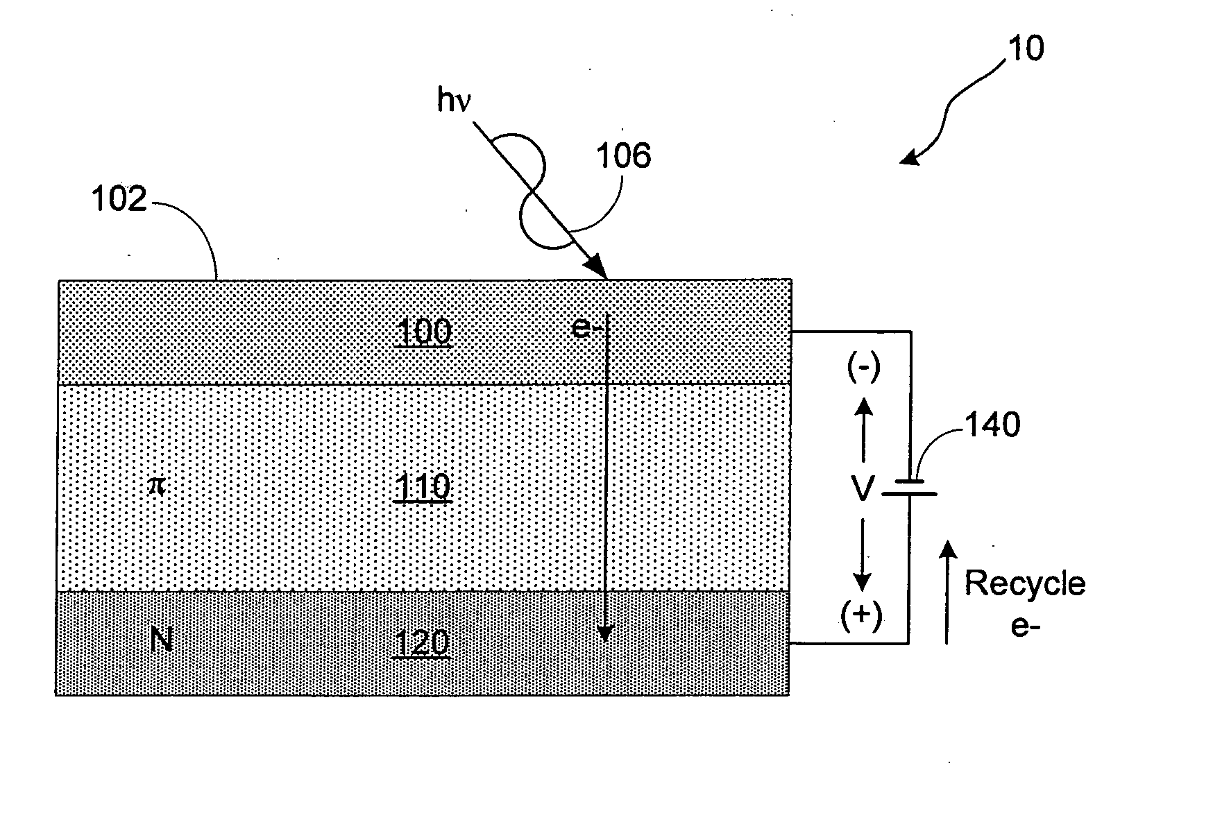
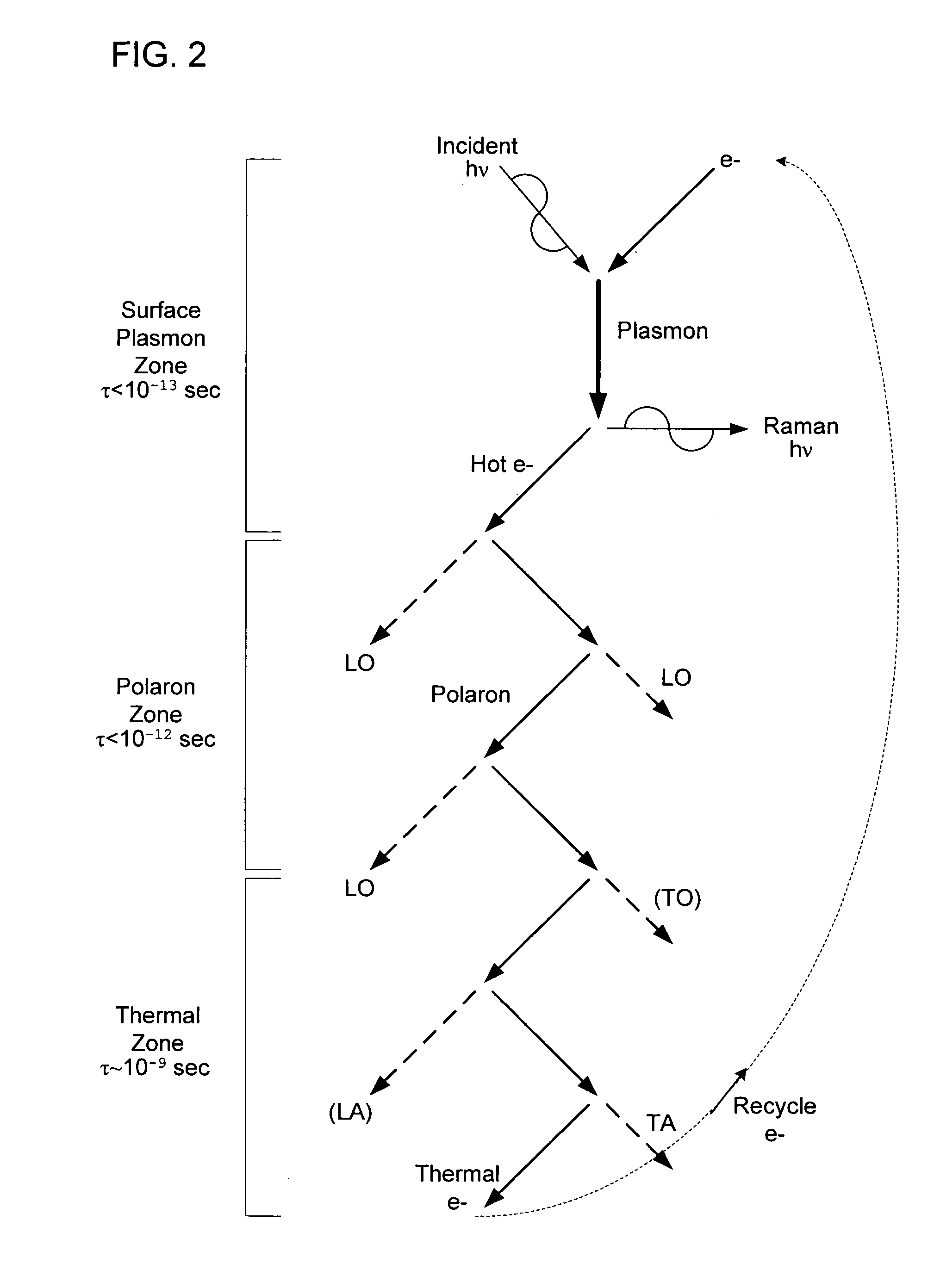
[0021] Referring to FIG. 2, a Feynman diagram depicts the decays scheme of a jellium or plasmon particle. An incident photon laser pulse that strikes a conductive mass of material (such as silver, gold, or other metal) excites free electrons to set up a plasmon, which then decays by emitting a high-energy electron and a Raman scattering photon that is reflected back from the mass. Thus, conservation of momentum dictates that the matching high-energy electron travels in a generally opposite direction from that of the Raman photon, and away from the surface. As the plasmon decays after the pulse, and accumulation underneath the surface of such high-energy “hot” electrons of energy between 0.04 eV and 12 eV begins to collapse towards the interior of the conductive material and proceed to interact with the ionic lattice atoms of this material. If this material is polar (that is, strongly ionic in nature), these high-energy electrons are quickly quenched. This stream of high-energy elect...


PUM

PropertyMeasurementUnit
plasmon frequenciesaaaaaaaaaa
energyaaaaaaaaaa

Abstract

An integrated plasmon detector includes a top layer of material adapted to generate a plasmon when excited by a beam of light incident onto a surface of the top layer, an interface layer joined to the top layer opposite from the surface of the top layer and adapted to slow polarons emitted by the plasmon to thermal electrons, and a collector layer joined to the interface layer opposite from the top layer and adapted to collect the thermal electrons from the interface layer.

Description

CROSS-REFERENCE TO RELATED APPLICATIONS [0001] This application claims the benefit of U.S. provisional Patent Application Ser. No. 60 / 602,117, filed Aug. 17, 2004 for “Using a Polaron Interaction Zone as an Interface to Integrate a Surface Plasmon Layer and a Semiconductor Detector” and U.S. provisional Patent Application Ser. No. 60 / 602,061, filed Aug. 17, 2004 for “Utilizing an Integrated Plasmon Detector to Measure a Metal Deposit Roughness on a Semiconductor Surface,” both by David T. Wei and Axel Scherer, the disclosures of which are incorporated in their entirety herein by reference thereto. This application is filed on the same day as U.S. patent application No. ______ Attorney Docket No. 622688, for “Utilizing an Integrated Plasmon Detector to Measure a Metal Deposit Roughness on a Semiconductor Surface”, also incorporated herein by reference in its entirety. STATEMENT REGARDING FEDERALLY SPONSORED RESEARCH OR DEVELOPMENT [0002] The present invention was supported in part by...

Claims


Application Information

Patent Timeline
Patent Type & Authority Applications(United States)
IPC IPC(8): G01N21/55
CPCG01B11/303G01N21/553G01N21/658G01N2021/1719H01L49/00H10N99/00
Inventor WEI, DAVID T.SCHERER, AXEL
Owner CALIFORNIA INST OF TECH
Why Eureka
Try Eureka