Memory using mixed valence conductive oxides

a technology of conductive oxides and mixed valence, applied in the field of nonvolatile memory, can solve the problems of complex forming process, inherently variable, and inability to achieve consistent device characteristics or long-term stability, and no one has successfully implemented a metal-insulator-metal structure into a commercial solid-state memory devi

Inactive Publication Date: 2006-08-03
UNITY SEMICON
View PDF33 Cites 292 Cited by
  • Summary
  • Abstract
  • Description
  • Claims
  • Application Information

AI Technical Summary

Problems solved by technology

However, nobody has successfully implemented a metal-insulator-metal structure into a commercial solid-state memory device.
However, the authors caution, “The forming process is complex and inherently variable.
Also tunneling barriers are susceptible to changes in their characteristics w

Method used


Image

  • Memory using mixed valence conductive oxides
  • Memory using mixed valence conductive oxides
  • Memory using mixed valence conductive oxides

Examples


Embodiment Construction

[0031] In the following description, numerous specific details are set forth to provide a thorough understanding of the present invention. It will be apparent, however, to one skilled in the art that the present invention may be practiced without some or all of these specific details. In other instances, well known process steps have not been described in detail in order to avoid unnecessarily obscuring the present invention.

The Memory Array

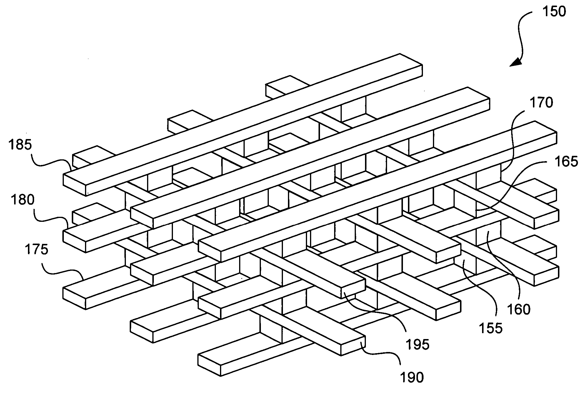
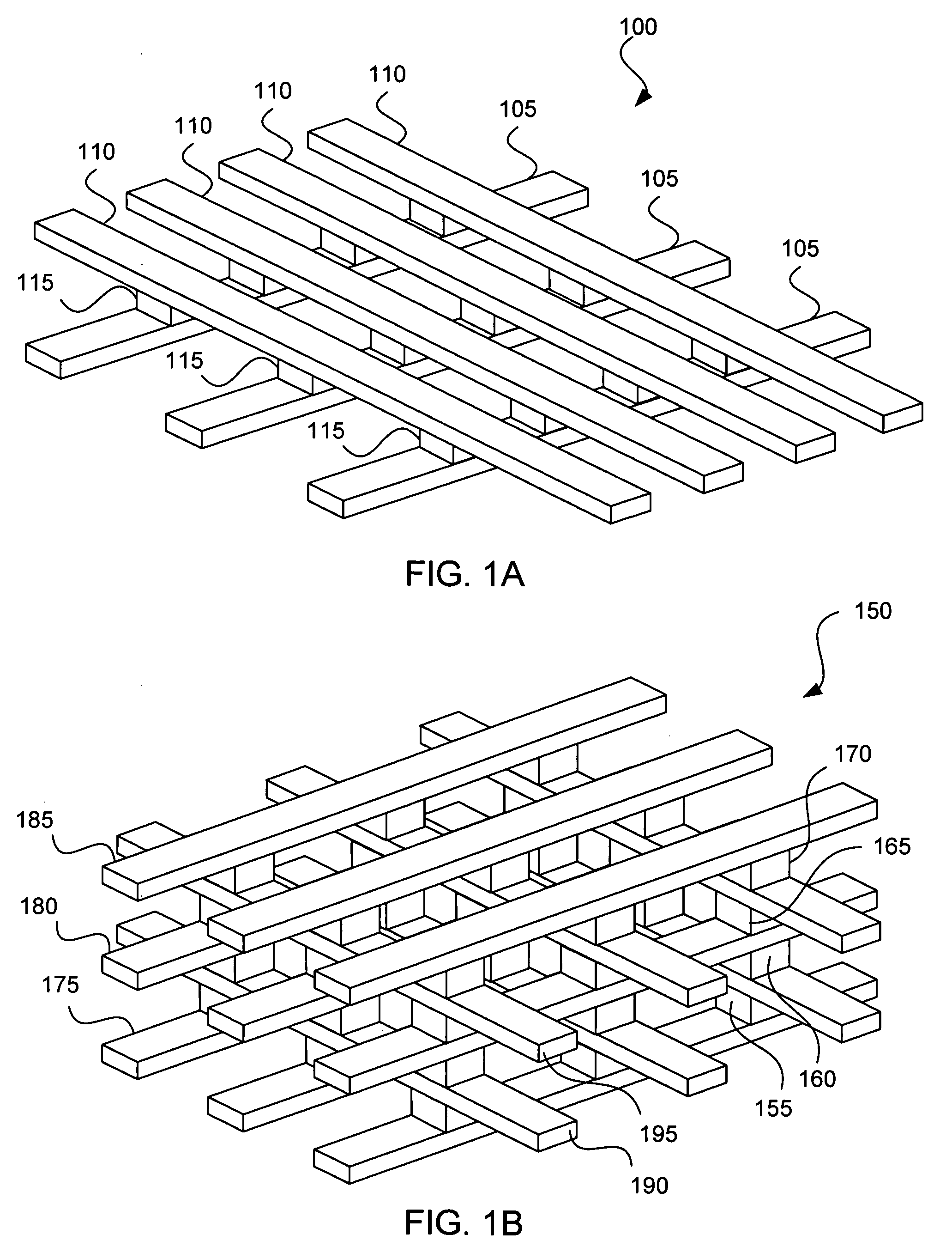
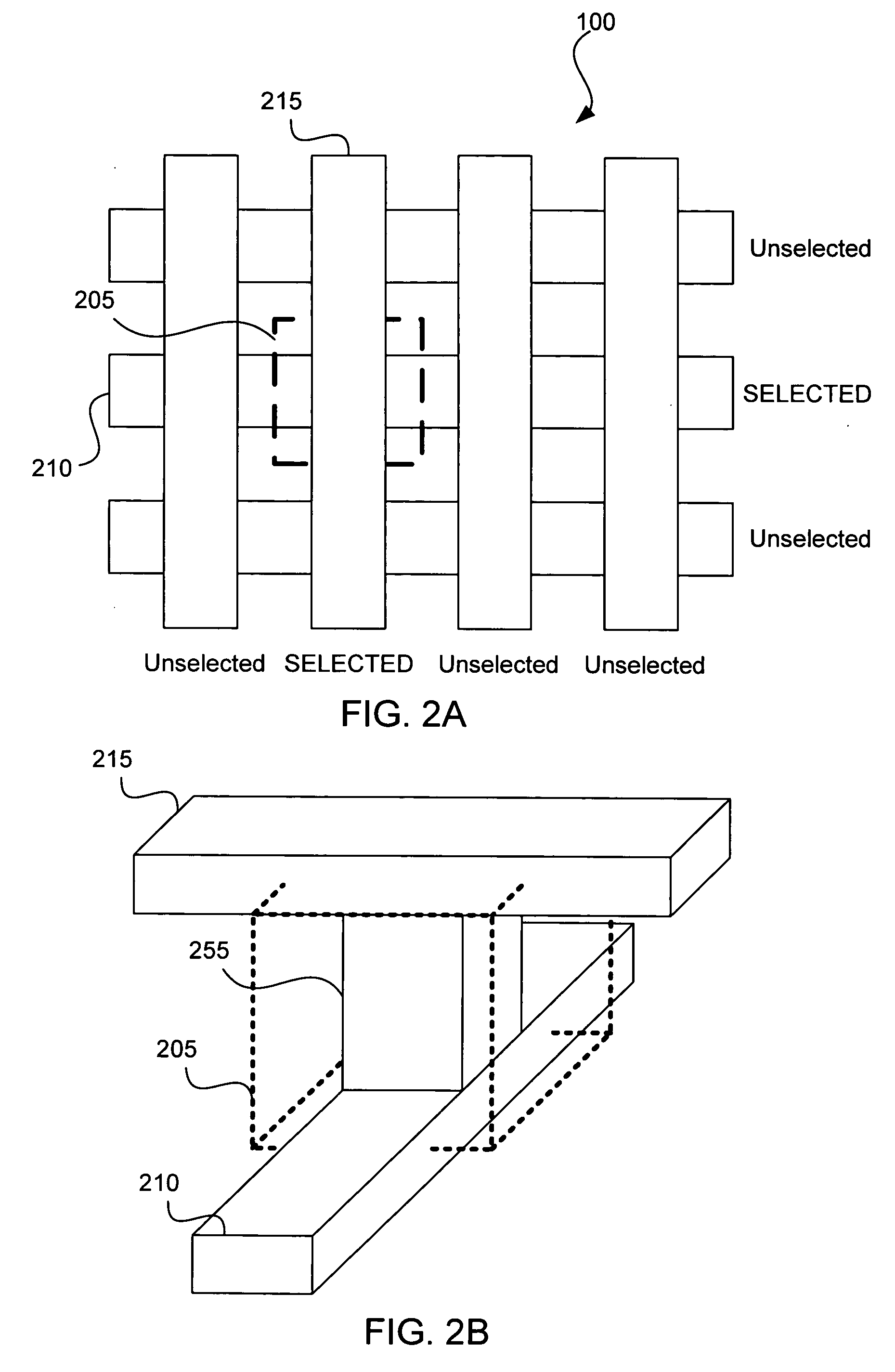
[0032] Conventional nonvolatile memory requires three terminal MOSFET-based devices. The layout of such devices is not ideal, usually requiring an area of at least 8 f2 for each memory cell, where f is the minimum feature size. However, not all memory elements require three terminals. If, for example, a memory element is capable of changing its electrical properties (e.g., resistivity) in response to a voltage pulse, only two terminals are required. With only two terminals, a cross point array layout that allows a single cell to be fabricated ...


PUM


Abstract

A memory using a mixed valence conductive oxides. The memory includes a mixed valence conductive oxide that is less conductive in its oxygen deficient state and a mixed electronic ionic conductor that is an electrolyte to oxygen and promotes an electric field effective to cause oxygen ionic motion.

Description

CROSS-REFERENCE TO RELATED APPLICATIONS [0001] This application is a continuation of “Memory Using Variable Tunnel Barrier Widths,” U.S. application Ser. No. 10 / 934,951, filed Sep. 3, 2004, which is incorporated herein by reference in its entirety and for all purposes.BACKGROUND OF THE INVENTION [0002] 1. Field of the Invention [0003] The present invention relates to computer memory and more specifically to non-volatile memory. [0004] 2. Description of the Related Art [0005] Memory can either be classified as volatile or nonvolatile. Volatile memory is memory that loses its contents when the power is turned off. In contrast, non-volatile memory does not require a continuous power supply to retain information. Most non-volatile memories use solid-state memory devices as memory elements. [0006] Since the 1960s, a large body of literature has evolved that describes switching and memory effects in metal-insulator-metal structures with thin insulators. One of the seminal works was “New C...

Claims


Application Information

Patent Timeline
IPC IPC(8): G11C11/34
CPCG06F17/5045H01L45/1253G11C13/0007G11C13/0009G11C2213/11G11C2213/31G11C2213/32G11C2213/53G11C2213/54G11C2213/56G11C2213/71G11C2213/79H01L45/1625H01L45/08H01L45/1233H01L45/146H01L45/147H01L27/2436H01L27/2481G11C13/004G11C13/0069G11C2013/0045G11C2013/005G11C2013/009H01L45/085G11C11/5685G06F30/30H10B63/30H10B63/84H10N70/24H10N70/8836H10N70/026H10N70/8833H10N70/826G11C16/02G11C11/42H10N70/245H10N70/828H10N70/841
Inventor RINERSON, DARRELLCHEVALLIER, CHRISTOPHE J.KINNEY, WAYNELAMBERTSON, ROYLONGCOR, STEVEN W.SANCHEZ, JOHN E. JR.SCHLOSS, LAWRENCESWAB, PHILIP F.S.WARD, EDMOND
Owner UNITY SEMICON
Why Eureka
Try Eureka