
Field effect transistor and method of manufacturing a field effect transistor

a field effect transistor and transistor technology, applied in the field of field effect transistors, to achieve the effect of reducing the on-resistance of the amplifying element, and limiting the chronological change of the set curren

Inactive Publication Date: 2006-08-10
NEC ELECTRONICS CORP
View PDF2 Cites 27 Cited by
  • Summary
  • Abstract
  • Description
  • Claims
  • Application Information

AI Technical Summary

Benefits of technology

[0012] Referring to FIG. 12, the electric field intensity in the drain diffusion layer is dispersed not only in the gate end region 124 but also in the region 126 located immediately under the FP electrode lower-end 118a at the drain electrode 120 side (hereafter referred to as FP end region), so that the electric field concentration on the gate end region 124 is restrained.
[0016] Therefore, a field effect transistor has been demanded having a field plate electrode with ensured breakdown voltage BVdss, with restrained chronological change in the set current, and with reduced on-resistance of the amplifying element.
[0018] According to this field effect transistor, the breakdown voltage BVdss is ensured; the chronological change in the set current is restrained; and the on-resistance of the amplifying element is reduced.
[0020] According to the present invention, the field plate electrode is disposed so that the distance of the field plate electrode spaced apart from the semiconductor substrate increases according as it goes along a direction from the gate electrode towards the drain electrode. Therefore, a field effect transistor can be provided with reduced on-resistance of the amplifying element, with ensured breakdown voltage BVdss, and with restrained chronological change in the set current. Therefore, the field effect transistor is excellent in the long-term reliability as an amplifying element of a high-frequency power amplifier.

Problems solved by technology

A conventional lateral-type MOSFET raises a problem in that an electric field is concentrated on a neighborhood of the drain-side end of the gate electrode in a diffusion layer.
This leads to chronological change in the set current Idq that passes at the time of bias application of the FET, causing an erroneous operation.

Method used


Image

  • Field effect transistor and method of manufacturing a field effect transistor
  • Field effect transistor and method of manufacturing a field effect transistor
  • Field effect transistor and method of manufacturing a field effect transistor

Examples


Embodiment Construction

[0036] The invention will be now described herein with reference to illustrative embodiments. Those skilled in the art will recognize that many alternative embodiments can be accomplished using the teachings of the present invention and that the invention is not limited to the embodiments illustrated for explanatory purposed.

[0037] Hereafter, embodiments of the present invention will be described with reference to the attached drawings. In all of the drawings, similar constituent elements will be denoted with similar symbols, and the explanation thereof will not be described at appropriate times.

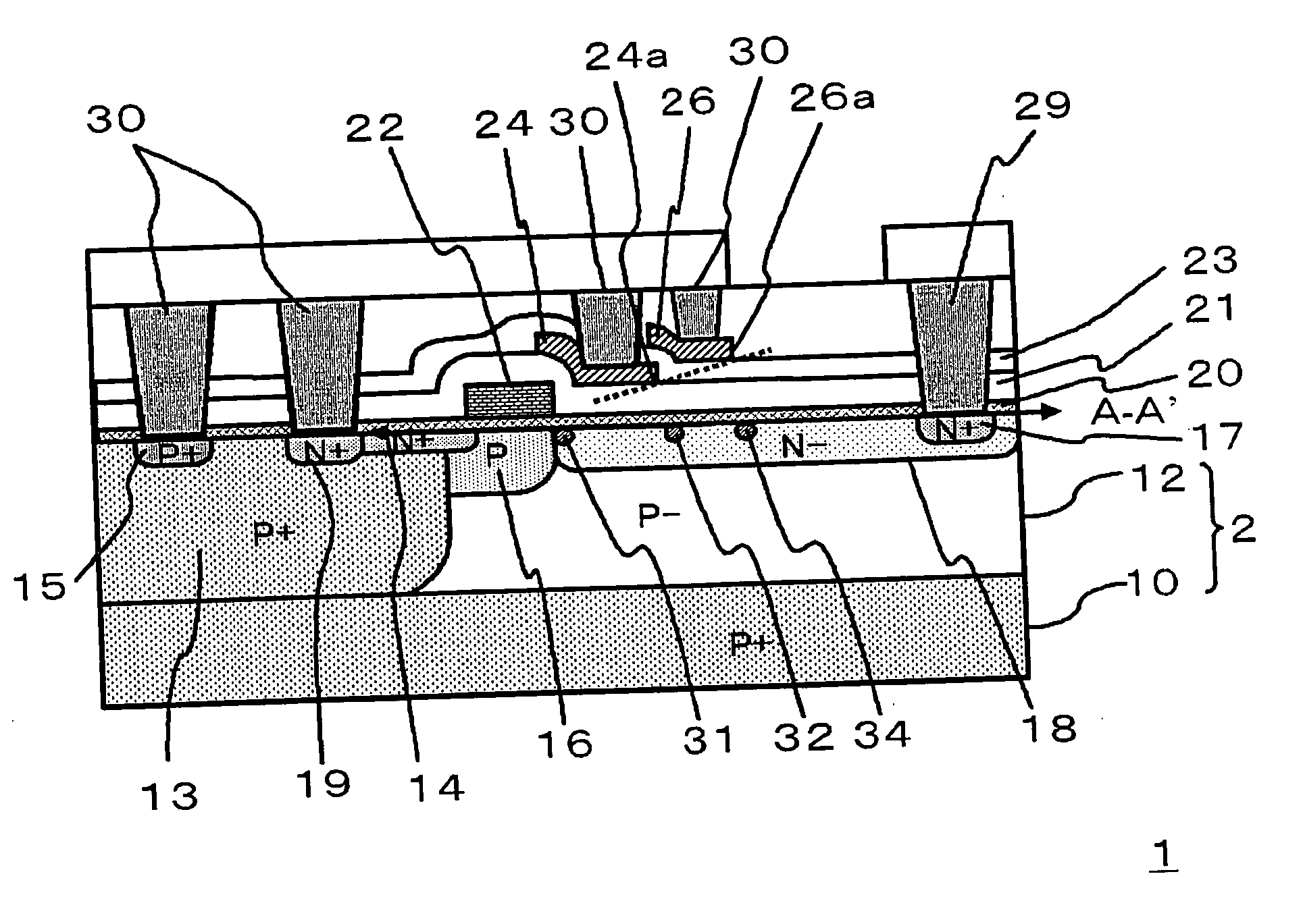
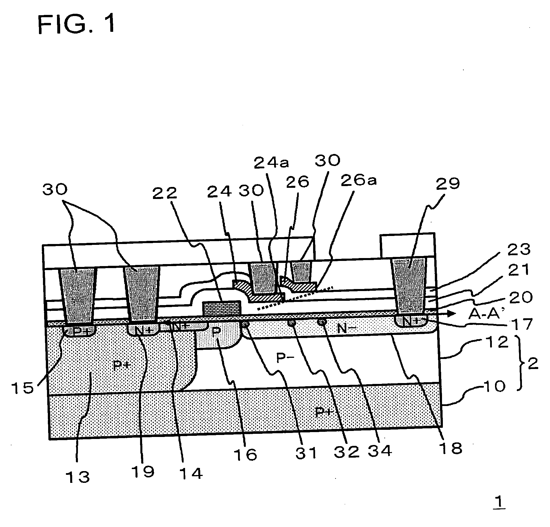
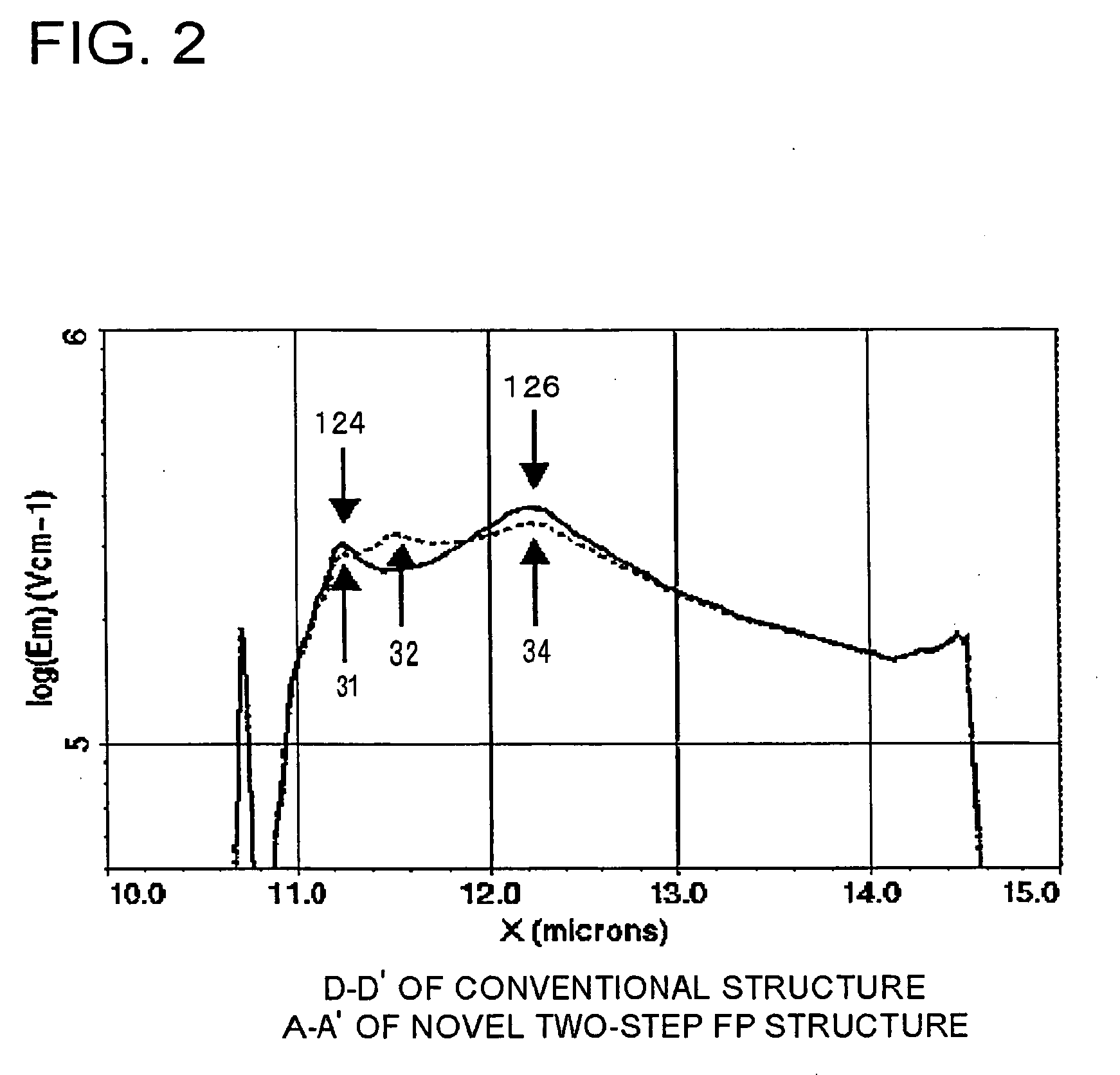
[0038]FIG. 1 is a schematic cross-sectional view illustrating the first embodiment of a field effect transistor according to the present invention, namely, a lateral-type MOSFET for high-frequency power amplification (hereafter simply referred to as “lateral power MOSFET”).

[0039] Referring to FIG. 1, a lateral power MOSFET 1 includes a source electrode 30 and a drain electrode 29 formed t...


PUM


Abstract

A field effect transistor includes a source electrode (30) and a drain electrode (29) formed to be spaced apart from each other on a semiconductor substrate (2), a gate electrode (22) disposed between the source electrode (30) and the drain electrode (29), and a field plate electrode (24, 26) disposed via an insulating film (21) above the semiconductor substrate (2) in a region between the gate electrode (22) and the drain electrode (29), wherein a surface of the semiconductor substrate (2) is flat, and a distance between the semiconductor substrate (2) and the field plate electrode (24, 26) increases according as it goes along a direction from the gate electrode (22) towards the drain electrode (29). With this field effect transistor, the breakdown voltage BVdss is ensured; the chronological change in the set current is restrained; and the on-resistance of an amplifying element is reduced.

Description

[0001] This application is based on Japanese Patent application NO. 2005-035209, the content of which is incorporated hereinto by reference. BACKGROUND [0002] 1. Technical Field [0003] The present invention relates to a field effect transistor having a field plate electrode and a method of manufacturing the same. [0004] 2. Related Art [0005] For W-CDMA (Wideband-Code Division Multiple Access) use, there is an increasing demand for higher performance and downsizing of high-frequency power amplifiers. Since a power supply voltage of 28V is used in base stations, about 80V is needed for a breakdown voltage BVdss between the drain and the source (hereafter simply referred to as “breakdown voltage BVdss”) as a performance of amplification elements of a high-frequency power amplifier. Also, since a large power of 280 W or more is required as a high-frequency power output, it is necessary to achieve a higher output per chip by reducing the on-resistance of the amplifying element in realizi...

Claims


Application Information

Patent Timeline
Patent Type & Authority Applications(United States)
IPC IPC(8): H01L29/76
CPCH01L21/31111H01L21/31116H01L21/31155H01L29/402H01L29/404H01L29/41758H01L29/66659H01L29/7835
Inventor TSUBAKI, SHIGEKI
Owner NEC ELECTRONICS CORP
Features
  • Generate Ideas
  • Intellectual Property
  • Life Sciences
  • Materials
  • Tech Scout
  • Unparalleled Data Quality
  • Higher Quality Content
  • 60% Fewer Hallucinations
Learn More