Semiconductor apparatus with crosstalk noise reduction circuit

a technology of crosstalk noise reduction and semiconductor devices, which is applied in the direction of television system scanning details, radio control devices, television systems, etc., can solve the problems of crosstalk between signal wires and a misoperation, the second control signal sometimes changes unintentionally, and the control signal in a pixel does not disclose crosstalk between control signals, so as to prevent the increase of the chip area

Inactive Publication Date: 2006-08-10
SOCIONEXT INC
View PDF4 Cites 8 Cited by
  • Summary
  • Abstract
  • Description
  • Claims
  • Application Information

AI Technical Summary

Benefits of technology

[0022] Thus, a mis-operation due to crosstalk can be preve

Problems solved by technology

Such a semiconductor apparatus always has the problem of crosstalk between signal wires and a mis-operation due to it.
When the control signal of the first control wire in the pixel changes, crosstalk noise occurs in the second control signal wire installed adjacently to the first control wire, and the second control signal sometimes changes unintentionally.
Although as to noise in an image sensor, it discloses reset noise caused when initializing sign

Method used


Image

  • Semiconductor apparatus with crosstalk noise reduction circuit
  • Semiconductor apparatus with crosstalk noise reduction circuit
  • Semiconductor apparatus with crosstalk noise reduction circuit

Examples


Embodiment Construction

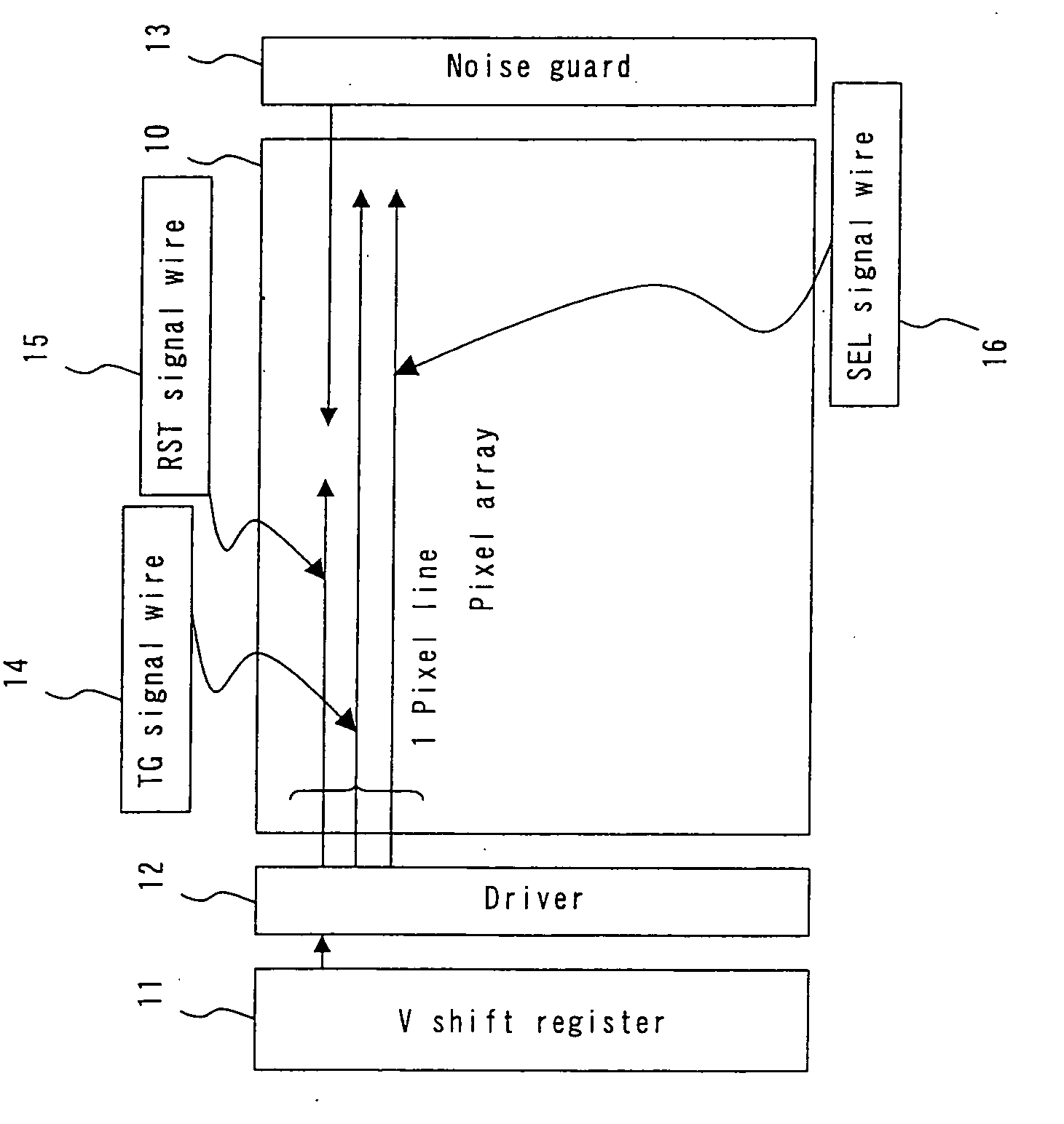
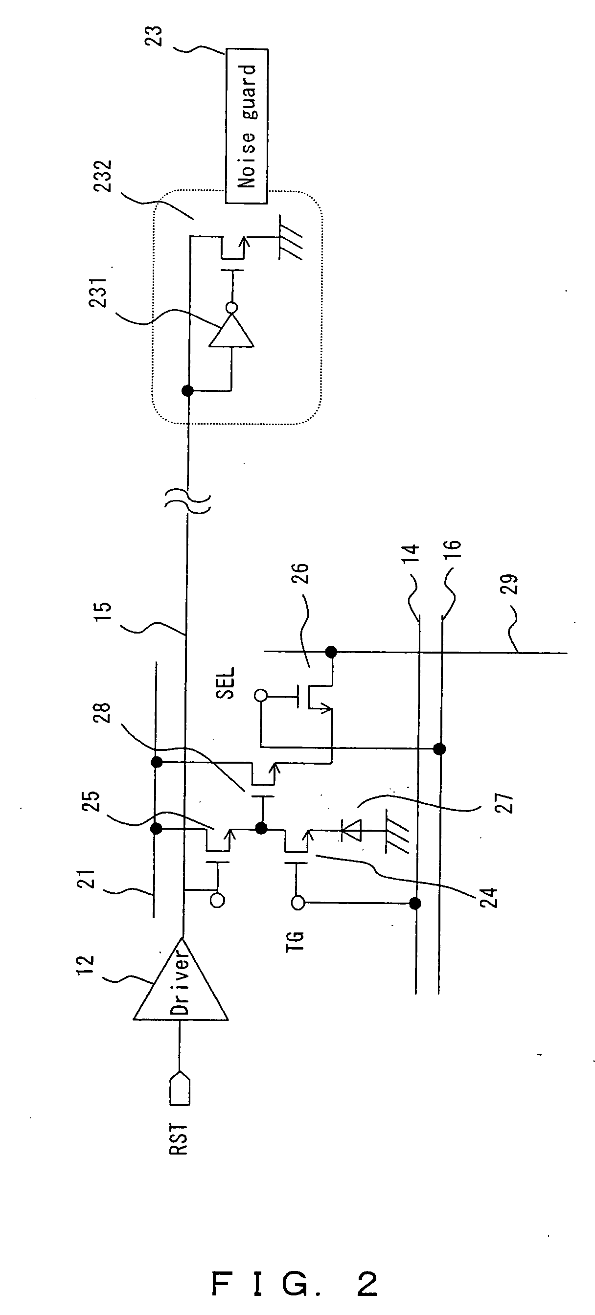
[0029] The present invention is described below using a solid-state image sensing device as an example of the semiconductor apparatus, and both a reset signal wire for resetting a stored pixel and a transfer gate signal wire for controlling the transfer of charge stored in a pixel as examples of the control signal wires.

[0030]FIG. 1 shows the basic configuration of the present invention. A V shift register 11 for selecting a pixel located in the vertical direction and the driver 12 of a control signal wire are disposed on one side of a pixel array 10 and a noise guard 13 is disposed on the other side. As the control signal wires, a transfer gate (TG) signal wire 14, a reset (RST) signal wire 15 and a selection (SEL) signal wire 16 are described. Only the reset signal wire 15 is connected to the noise guard 13.

[0031] The reset signal wire 15 is divided into an arrow line from the driver side and an arrow line from the noise guard side. This indicates that in the present invention, ...


PUM


Abstract

In order to reduce crosstalk caused between control signal wires in a semiconductor apparatus without increasing the size of the semiconductor apparatus, a noise guard circuit is provided at the opposite end of the control signal wire to the driver circuit. The noise guard circuit controls in such a way as to increase the impedance between the relevant control signal wire and a fixed potential when the logic of the relevant control signal wire is positive logic for driving the element, and as to decrease the impedance between the relevant control signal wire and a fixed potential when the logic of the relevant control signal wire is negative logic for driving the element.

Description

CROSS REFERENCE TO RELATED APPLICATIONS [0001] This application is based upon and claims the benefit of priority from the prior Japanese Patent Application No. 2005-028446, filed on Feb. 4, 2005, the entire contents of which are incorporated herein by reference. BACKGROUND OF THE INVENTION [0002] 1. Field of the Invention [0003] The present invention relates to a technology for reducing crosstalk noise between signal wires in a semiconductor apparatus, such as a solid-state image sensing device and the like. [0004] 2. Description of the Prior Art [0005] Some semiconductor apparatus, such as a solid-state image sensing device, a liquid crystal displaying device, semiconductor memory and the like, comprises a plurality of driver circuits, a plurality of types of control signal wires connected to the driver circuits, for transmitting control signals and a group of elements which are connected to the plurality of types of control signal wires and driven by the driver circuits. [0006] Su...

Claims


Application Information

Patent Timeline
IPC IPC(8): H04N5/335H01L27/146H04N5/341H04N5/359H04N5/369H04N5/374H04N5/376
CPCH01L27/14609H04N5/3577H04N25/617H04N25/62
Inventor FUNAKOSHI, JUNHIGUCHI, TSUYOSHI
Owner SOCIONEXT INC
Why Eureka
Try Eureka