Thin-film transistor and method for manufacturing the same

a thin-film transistor and manufacturing method technology, applied in the field of thin-film transistors, can solve the problems of large-scale devices, high manufacturing cost of tft, and high cost of tft manufacturing, and achieve the effects of high carrier mobility, low cost process, and superior mechanical flexibility and impact resistan

Active Publication Date: 2006-08-10
PANASONIC CORP
View PDF5 Cites 8 Cited by
  • Summary
  • Abstract
  • Description
  • Claims
  • Application Information

AI Technical Summary

Benefits of technology

[0009] A primary object of the present invention is to provide a TFT which is formed by low cost process, is superior in mechanical flexibility and impact resistance and has high carrier mobility, and a method of manufacturing the same.

Problems solved by technology

However, the process of manufacturing TFT using these semiconductive materials and insulation materials requires large-scale devices for plasma CVD method and expensive thin-film control devices for high-precision process.
For this reason, a manufacturing cost of the TFT becomes high.
Further, available substrate materials are limited because the above-mentioned plasma CVD method typically includes a step using processing temperature of higher than 350° C.
However, the organic semiconductor currently reported is lower in carrier mobility than inorganic semiconductors such as amorphous silicon and low-temperature polysilicon.
This can not be realized by the above-mentioned low-cost process.
Therefore, the latter is light but it has problem in reliability of mechanical flexibility and impact resistance.
That means, when TFT is formed on a plastic substrate as a flexible substrate using an organic / inorganic hybrid semiconductive material, bending durability of TFT is extremely low, comparing with a case where TFT is formed of the organic semiconductor.

Method used


Image

  • Thin-film transistor and method for manufacturing the same
  • Thin-film transistor and method for manufacturing the same
  • Thin-film transistor and method for manufacturing the same

Examples


first embodiment

[0050] In the first embodiment of the present invention, TFT comprises a semiconductor layer made of organic semiconductive material which contains inorganic semiconductive material particles therein. Typical configurations, manufacturing methods, evaluation results and others will be explained.

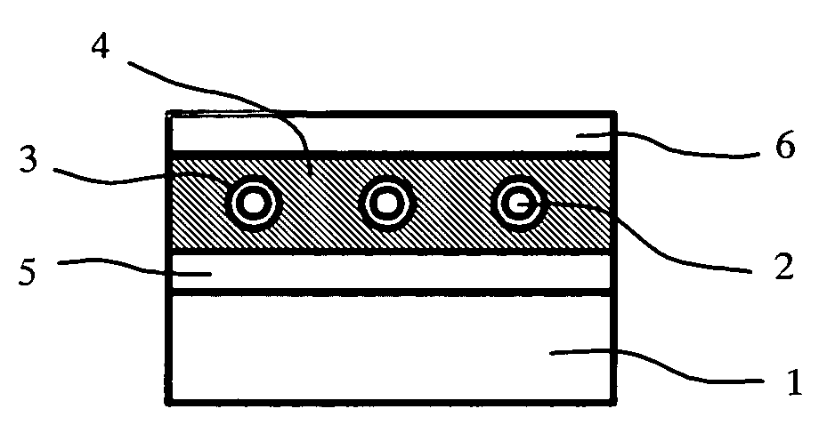
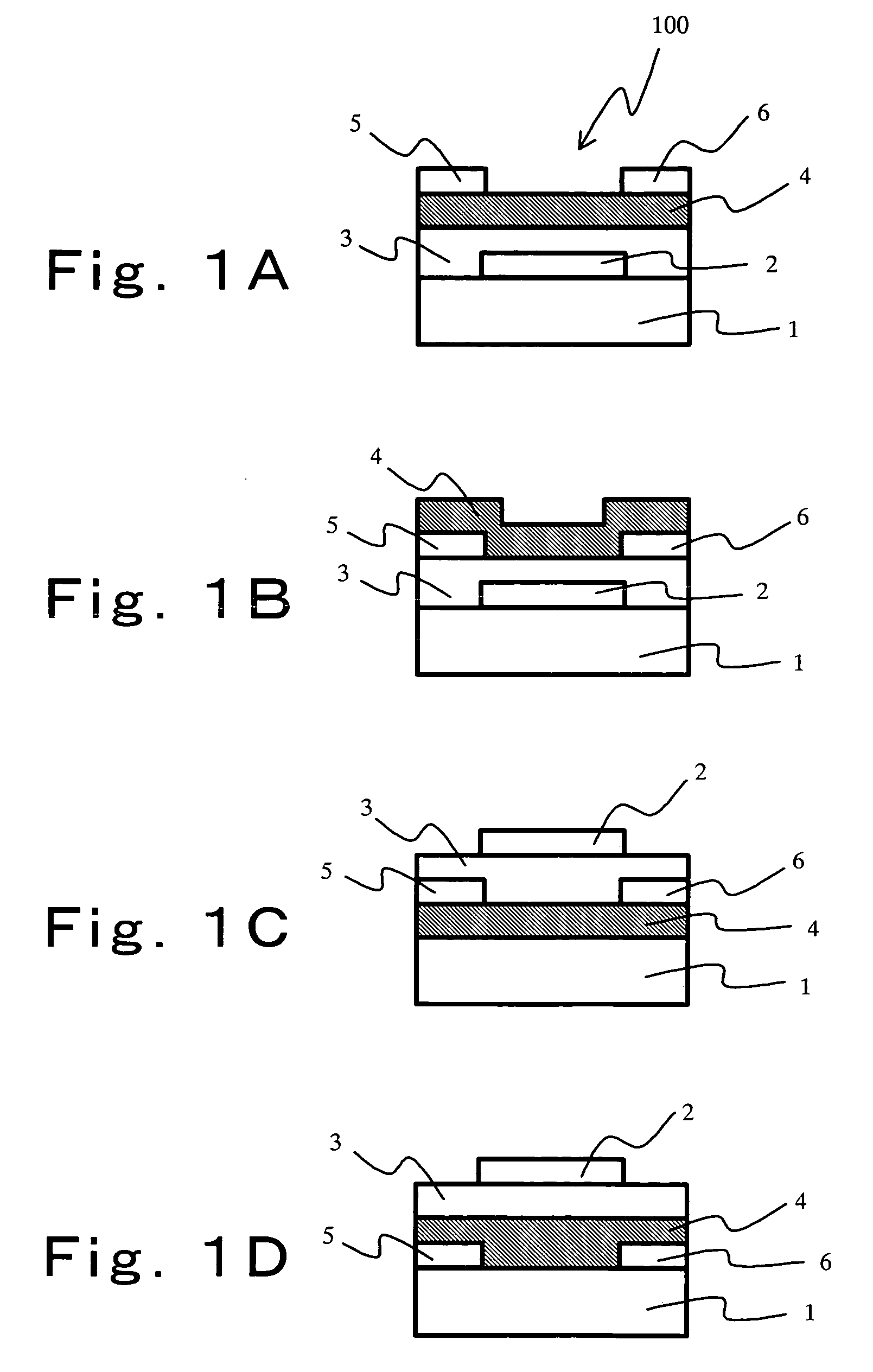
[0051]FIG. 1 is a sectional view schematically showing typical first configuration of TFT.

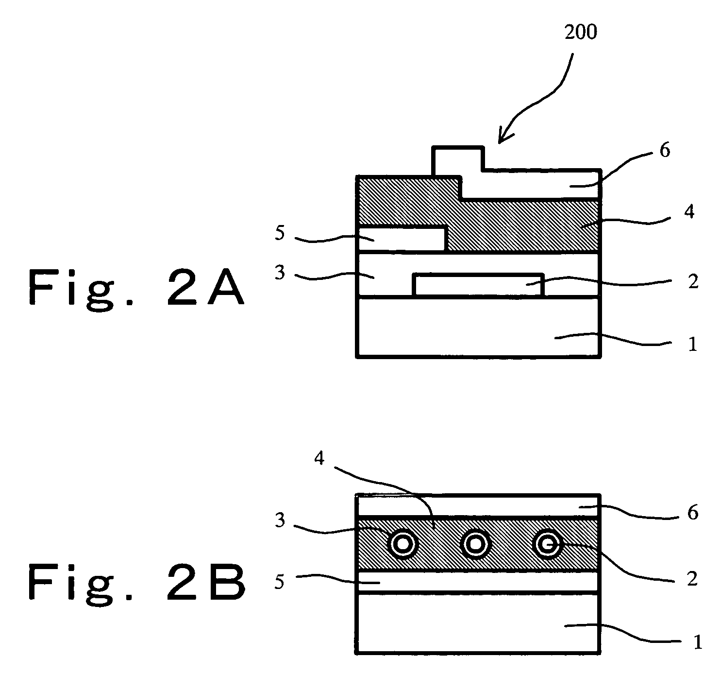
[0052] As shown in FIGS. 1A to 1D, a variety of configurations of TFT 100 of the present embodiment are considered. In any configuration, it is common that a substrate 1, a gate electrode 2, a gate insulating layer 3, a semiconductor layer 4, a source electrode 5, and a drain electrode 6 are comprised as constitution elements. Here, FIGS. 1A and 1B are called “bottom-gate method”. FIGS. 1C and 1D are called “top-gate method”. Further, FIGS. 1A and 1C are also called “top-contact method” and FIGS. 1B and 1D are also called “bottom-contact method”, depending on positional relation between the semiconduct...

second embodiment

[0091] In second embodiment of the present invention, TFT comprises a semiconductor layer made of organic semiconductive material which contains a plurality of inorganic conductive material particles therein. The typical configuration, manufacturing method, and evaluation result and others will be explained.

[0092] In this embodiment, the configuration of TFT itself is the same as that of the first embodiment shown in FIG. 1C. Polyethylene plastic substrate is used as material of substrate 1. Substituted oligothiophene is used as an organic semiconductive material of semiconductor layer 4 and particulate Cu is used as inorganic conductive material to be dispersed inside the semiconductor layer. The PEDOT-based electrode material is used as material of a source electrode 5, a drain electrode 6 and a gate electrode 2. And polyvinyl phenol is used as material of a gate insulating layer 3.

[0093] A method of manufacturing TFT of this embodiment is basically the same as that of the first...

third embodiment

[0101] In third embodiment, TFT comprises a semiconductor layer made of organic semiconductive material which contains a plurality of inorganic semiconductive material particles and inorganic conductive material particles therein. In this embodiment, the sample configuration for evaluating semiconductor property, and manufacturing method of TFT are same as in the first embodiment and second embodiment. Therefore, explanation will be omitted. And material applied to each configuration element of TFT, except for semiconductor layer, is same as the first embodiment. For example, the organic semiconductive material which is based to form the semiconductor layer is oligothiophene as in the first embodiment.

[0102] Now, the evaluation result with regard to the semiconductor property of TFT in this embodiment will be explained.

[0103]FIG. 13 is a comparative diagram showing comparison among kinds of inorganic semiconductive material and inorganic conductive material, each particle diameter...


PUM

PropertyMeasurementUnit
temperatureaaaaaaaaaa
sizeaaaaaaaaaa
channel lengthaaaaaaaaaa

Abstract

A thin-film transistor (100) of the present invention comprises a semiconductor layer (4), and a source region (5), a drain region (6), and a gate region (2) which formed on the semiconductor layer to be separated from each other. Said semiconductor layer is made of composite material, and said composite material comprises organic semiconductive material and at least one kind of inorganic material particles dispersed inside the organic semiconductive material.

Description

TECHNICAL FIELD [0001] The present invention relates to a thin-film transistor and a method for manufacturing the same, and particularly to a thin-film transistor wherein inorganic material particles are dispersed inside an organic semiconductor to form a semiconductor layer, and a method for manufacturing the same. BACKGROUND ART [0002] At present, a thin-film transistor (hereinafter referred to as TFT) is suitably used as a drive element in an active matrix liquid crystal display and the like. Various configurations of TFT have been proposed. However, basically, electric current flowing between a source electrode and a drain electrode which are in contact with a semiconductor layer is controlled by voltage (i.e. an electric field produced by applied voltage) applied to a gate electrode which is provided for the semiconductor layer with an insulating layer interposed between them. With regard to the semiconductor layer of TFT, a semiconductive material in practical use at present i...

Claims


Application Information

Patent Timeline
Patent Type & Authority Applications(United States)
IPC IPC(8): H01L21/84H01L27/148H01L21/336H01L29/786H01L51/00
CPCH01L51/0068H01L51/0566H01L2924/0002H01L2924/00H10K85/655H10K10/488
Inventor TAKEUCHI, TAKAYUKINANAI, NORISHIGE
Owner PANASONIC CORP
Why Eureka
Try Eureka