Precursor, thin layer prepared including the precursor, method of preparing the thin layer and phase-change memory device

a technology of phase-change memory and precursor, which is applied in the direction of thermoelectric devices, electric/magnetic/electromagnetic heating, organic chemistry, etc., can solve the problem of limit in realizing higher integrated memory devices, and achieve the effect of reducing the reset current that may be applied to change the crystal structure, uniform thickness, and higher performan

Active Publication Date: 2006-08-17
SAMSUNG ELECTRONICS CO LTD
View PDF4 Cites 123 Cited by
  • Summary
  • Abstract
  • Description
  • Claims
  • Application Information

AI Technical Summary

Benefits of technology

[0021] By employing a precursor according to example embodiments of the present invention, a thin layer having more uniform thickness, suitable for various devices may be obtained by lower temperature deposition. For example, a thin layer, for example, a GST thin layer, obtained by employing a Te precursor may be doped with a 15-group compound (for example, N) and / or a 14-group compound (for example, Si), and thus the reset current that may be applied to change the crystal structure may be decreased. Accordingly, a phase-change memory device with higher performance may be realized.

Problems solved by technology

As a result, there may be a limit in realizing higher integrated memory devices.

Method used


Image

  • Precursor, thin layer prepared including the precursor, method of preparing the thin layer and phase-change memory device
  • Precursor, thin layer prepared including the precursor, method of preparing the thin layer and phase-change memory device
  • Precursor, thin layer prepared including the precursor, method of preparing the thin layer and phase-change memory device

Examples


example 1

[0067]

[0068] As in the reaction scheme I, 0.1 mole of hexamethyldisilazane solution and 0.2 mole of nBu-Li were mixed in 1000 ml of hexane at −78° C. and ambient pressure, and then the mixture was reacted for 4 hours at room temperature to obtain the compound represented by formula II′ above.

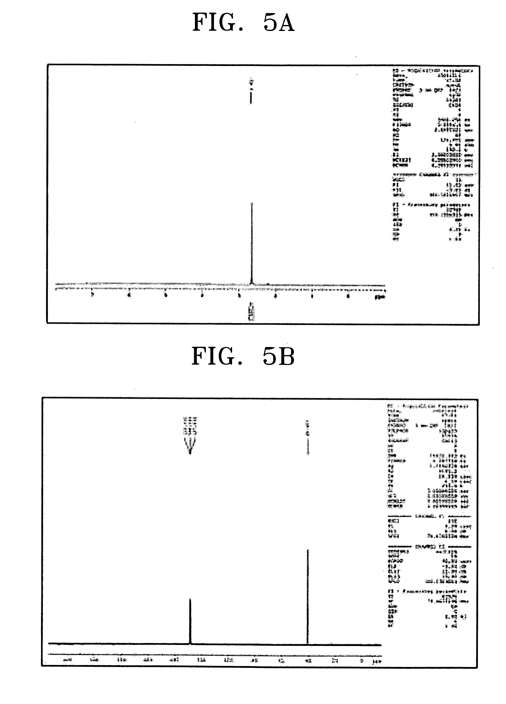
[0069] As in the reaction scheme II, 0.5 mole of the compound represented by the formula II′ and 0.5 mole of TeCl2 were mixed in 1000 ml of THF, and then the mixture was heated for 8 hours at 150° C. The mixture was evaporated at ambient temperature in a vacuum, fractional distillation was performed for synthesized Te precursor at 0.1 torr and 60° C. to obtain 24 g of the compound represented by formula II, e.g., Te[NH(Si(CH3)3)]2, and then 1H-NMR analysis and 13C-NMR analysis (all analysis was performed at C6D6 and 25° C.) were performed and the results are shown in FIGS. 5A and 5B, respectively. From FIGS. 5A and 5B, Te—N bond and N—Si bond of the compound of the formula II can be confirmed....

preparation example

Formation of a Layer Made of a GST Material and its Resistance Evaluation

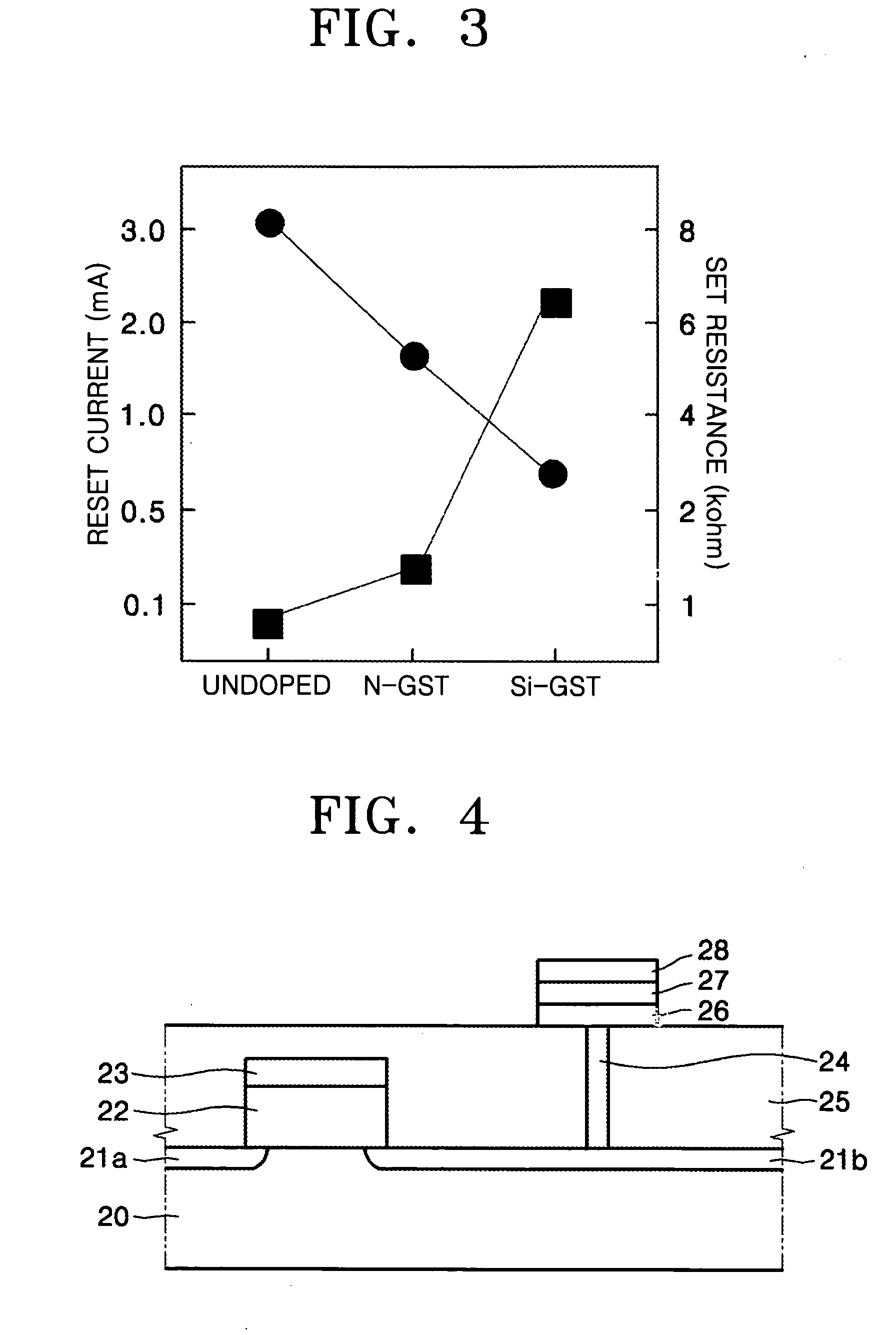
[0072] A Ge2Sb2Te5 layer doped with a 15-group compound (for example, N) and / or a 14-group compound (for example, Si) through the ALD process was formed by employing Ge[N(CH3)2]4 as a Ge precursor, Sb[N(Si(CH3)3)3] as a Sb precursor, and the Te precursor 1 as a Te precursor. The detailed conditions of the ALD process is the same as described in Table 1. Further, the Te / (Ge+Sb) cation ratio was controlled to be about 1.1,1.25, and 1.45. The resistance of the GST thin layer doped with a 15-group compound (for example, N) and / or a 14-group compound (for example, Si) obtained above was measured, and the results are shown in FIG. 7. According to FIG. 7, it can be seen that the resistance of the GST thin layer doped with a 15-group compound (for example, N) and / or a 14-group compound (for example, Si) decreases as Te / (Ge+Sb) cation ratio increases, that is, temperature increases.

[0073] The Te precursor for lower te...


PUM

PropertyMeasurementUnit
deposition temperatureaaaaaaaaaa
temperaturesaaaaaaaaaa
reset currentaaaaaaaaaa

Abstract

A Te precursor containing Te, a 15-group compound (for example, N) and/or a 14-group compound (for example, Si), a method of preparing the Te precursor, a Te-containing chalcogenide thin layer including the Te precursor, a method of preparing the thin layer; and a phase-change memory device. The Te precursor may be deposited at lower temperatures for forming a Te-containing chalcogenide thin layer doped with a 15-group compound (for example, N) and/or a 14-group compound (for example, Si). For example, the Te precursor may employ plasma enhanced chemical vapor deposition (PECVD) or plasma enhanced atomic layer deposition (PEALD) at lower deposition temperatures. The GST phase-change layer doped with a 15-group compound (for example, N) and/or a 14-group compound (for example, Si) formed by employing the Te precursor may have a decreased reset current, and thus when a memory device including the same is employed, its integration may be possible, and operation with higher capacity and/or higher speed may be possible.

Description

PRIORITY STATEMENT [0001] This application claims the benefit of Korean Patent Application No. 10-2005-0012037, filed on Feb. 14, 2005, in the Korean Intellectual Property Office, the disclosure of which is incorporated herein in its entirety by reference. BACKGROUND OF THE INVENTION [0002] 1. Field of the Invention [0003] Example embodiments of the present invention relate to a precursor, for example, a Te precursor, for lower temperature deposition, a thin layer, for example, a Te-containing chalcogenide thin layer, prepared by employing the precursor; and a method of preparing the thin layer, and for example, to a precursor for lower temperature deposition containing Te, a 15-group compound and / or a 14-group compound; a chalcogenide thin layer doped with a 15-group compound and / or a 14-group compound and prepared at lower temperature by employing the precursor, and a method of preparing the thin layer. Also, example embodiments of the present invention relate to a phase-change me...

Claims


Application Information

Patent Timeline
Patent Type & Authority Applications(United States)
IPC IPC(8): H01L29/08C07F7/10
CPCC07F7/10C23C16/305H01L27/2436H01L45/06H01L45/1233H01L45/144H01L45/1616H10B63/30H10N70/231H10N70/023H10N70/8828H10N70/826H05B6/6408
Inventor LEE, JUNG-HYUNKHANG, YOON-HO
Owner SAMSUNG ELECTRONICS CO LTD
Why Eureka
Try Eureka