Optical semiconductor device package and optical semiconductor device

a technology of optical semiconductor and semiconductor device, which is applied in the direction of semiconductor lasers, solid-state devices, lasers, etc., can solve the problems of reducing the flexibility of increasing the characteristic impedance, and deteriorating the reflection characteristics, so as to achieve the effect of widening the control range of the characteristic impedance of the lead and reducing the characteristic impedan

Inactive Publication Date: 2006-08-17
MITSUBISHI ELECTRIC CORP
View PDF6 Cites 10 Cited by
  • Summary
  • Abstract
  • Description
  • Claims
  • Application Information

AI Technical Summary

Benefits of technology

[0011] It is an object of this invention to provide an optical semiconductor device package and an optical semiconductor device in which characteristic impedance of a lead can be reduced, and a control range of the characteristic impedance of a lead can be widened.
[0013] By providing the impedance-adjusting dielectric substrate including at least one conductive layer and one dielectric layer laminated therein to cover at least portions facing the first and second leads on the plane part of the mounting base, the distance between the first and second leads and the mounting base is practically narrowed, or a structure equivalent to that is obtained, thereby reducing the characteristic impedances of the protruding parts from the stem main surface of the first and second leads. In addition, the characteristic impedance can be varied by changing the structure of the impedance-adjusting dielectric substrate. This allows greater flexibility and a wider range of control to the characteristic impedance.

Problems solved by technology

This causes an increase in characteristic impedance of the uncovered parts of the leads, and the resultant characteristic impedance mismatching causes an increase in reflection, thus deteriorating the reflection characteristics.
Therefore, only a low degree of flexibility and a limited range are given in controlling the characteristic impedances.

Method used


Image

  • Optical semiconductor device package and optical semiconductor device
  • Optical semiconductor device package and optical semiconductor device
  • Optical semiconductor device package and optical semiconductor device

Examples


Embodiment Construction

A. First Preferred Embodiment

[0026] An optical semiconductor device package according to a first preferred embodiment of this invention will be described with reference to FIGS. 1 to 4.

[0027]

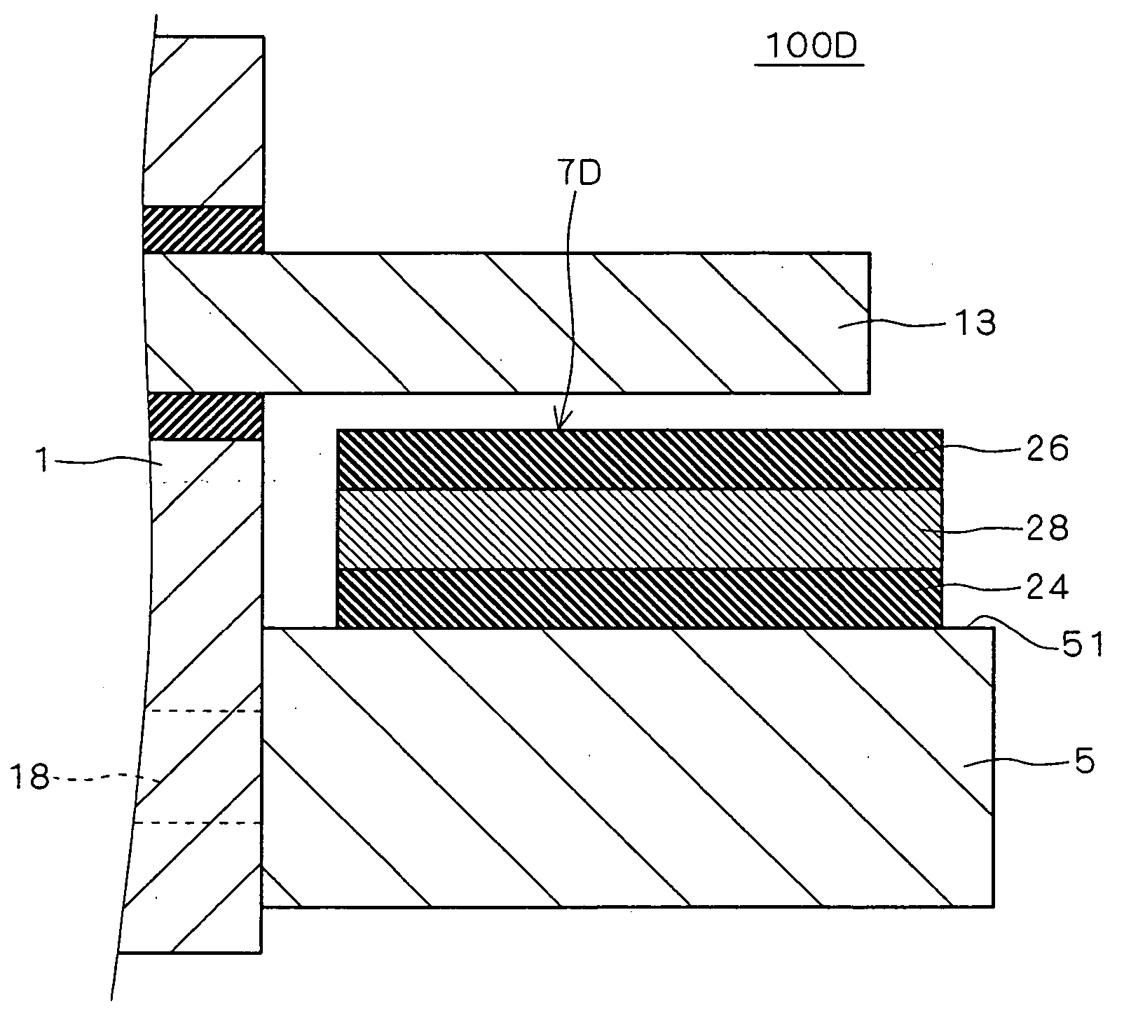
[0028]FIG. 1 is a perspective view of the general structure of an optical semiconductor device package 100 according to the first preferred embodiment.

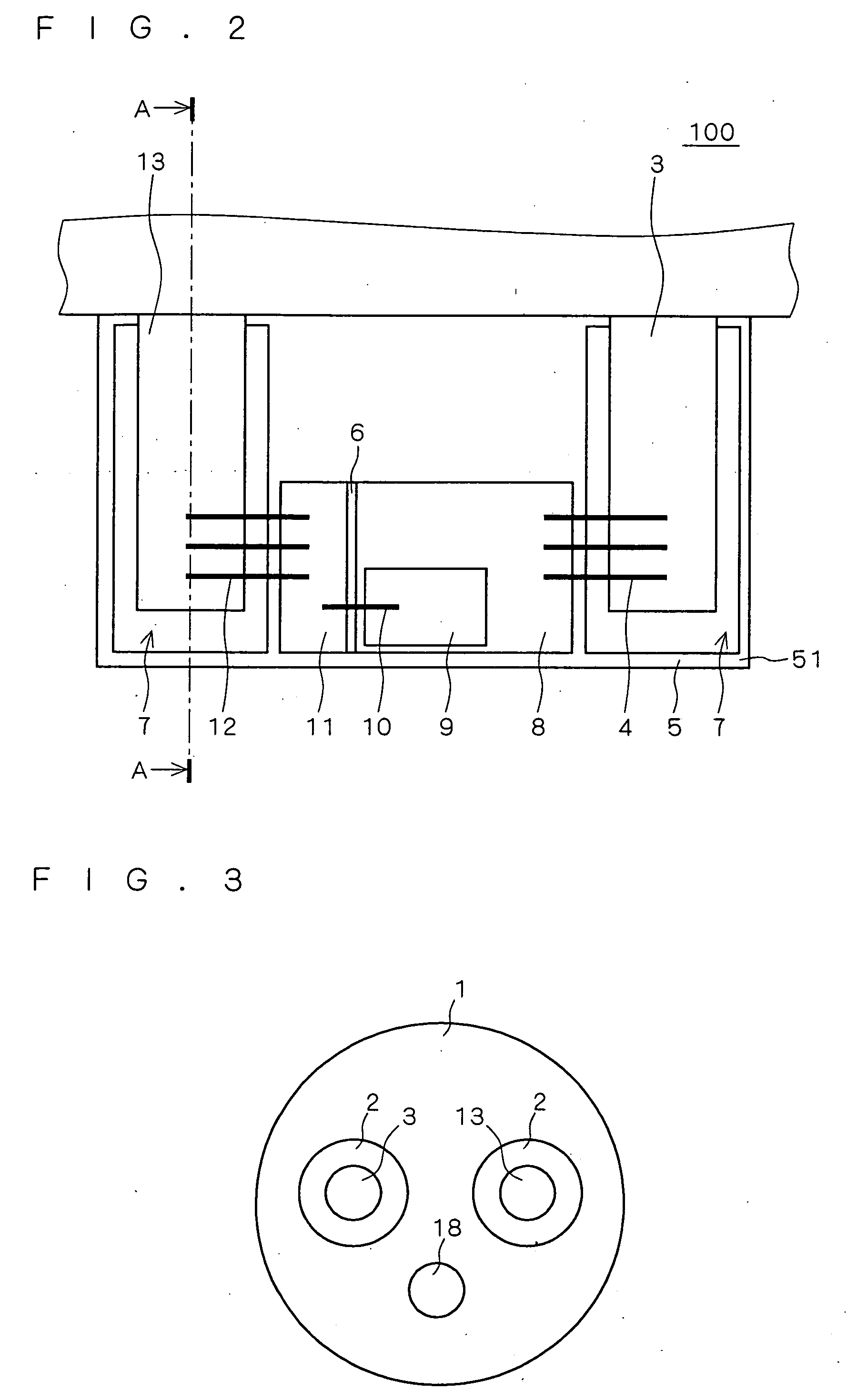
[0029] The optical semiconductor device package 100 is the so-called stem type optical semiconductor device package that includes a disc-shaped stem 1, metallic leads 3 and 13 (first and second leads) in rod form penetrating the stem 1 in the direction of the thickness to protrude from a main surface of the stem 1 and a mount 5 having a plane part 51 extending vertically from the main surface of the stem 1.

[0030] The mount 5 is a mounting base for an optical semiconductor chip 9, is made of a metal having good electrical conductivity and thermal conductivity, is in half-cylindrical form, for example, and has the plane part 51 facing the leads 3...


PUM


Abstract

An optical semiconductor device package includes a disc-shaped stem, metallic leads in rod form penetrating the stem in the direction of the thickness to protrude from a main surface of the stem, and a mount extending vertically from the main surface of the stem, with a plane part of the mount facing the leads. A dielectric substrate is mounted on the plane part, and an optical semiconductor chip is mounted thereon. Two impedance-adjusting dielectric substrates which are rectangular in plan view are provided extending in parallel with the leads, to cover the plane part facing the leads.

Description

BACKGROUND OF THE INVENTION [0001] 1. Field of the Invention [0002] This invention relates to optical semiconductor device packages and optical semiconductor devices housing optical semiconductor chips, and in particular to optical semiconductor device packages and optical semiconductor devices in which characteristic impedances of leads are reduced. [0003] 2. Description of the Background Art [0004] Recent years have seen an increase in transmission rate in optical communications, up to 10 Gbps or faster in some cases. With this, there have been demands for optical semiconductor chips as well as optical semiconductor device packages housing them that are relatively inexpensive and have excellent high frequency characteristics. [0005] As a structure that satisfies such demands, Japanese Patent Application Laid-Open No. 2004-311923 (FIG. 4) discloses a stem type optical semiconductor device package in coaxial form having a simple structure. [0006] The stem type refers to a structure ...

Claims


Application Information

Patent Timeline
Patent Type & Authority Applications(United States)
IPC IPC(8): H01L33/00H01S5/02315
CPCH01S5/02212H01S5/02236H01S5/02276H01S5/042H01L2224/48091H01L2224/48145H01L2924/00014H01L2924/3011H01L2924/00H01S5/0233H01S5/0235H01S5/02345H01S5/02315H01L2924/00012
Inventor YASUI, NOBUYUKI
Owner MITSUBISHI ELECTRIC CORP
Why Eureka
Try Eureka