Copper bonding wire for semiconductor packaging

a technology of copper bonding wire and semiconductor packaging, which is applied in the direction of packaging foodstuffs, packaging goods, transportation and packaging, etc., can solve the problems of high price of au, inability to meet the requirements of power ic devices, and ic packages, so as to improve the metal squeeze out of chip pads, shorten the tail of bonding wire, and improve the effect of chip cratering

Inactive Publication Date: 2006-08-24
MK ELECTRON
View PDF8 Cites 36 Cited by
  • Summary
  • Abstract
  • Description
  • Claims
  • Application Information

AI Technical Summary

Benefits of technology

[0017] The present invention provides a copper bonding wire for semiconductor packaging for ...

Problems solved by technology

However, Au is high-priced and does not satisfy requirements of power IC devices and ultrahigh speed IC packages having recently been developed in terms of electrical property.
In spite of these advantages, Cu has a poorer oxidation resistance than Au and is harder than Au.
Thus, it is difficult for Cu to replace Au in terms of bonding wire.
The short tail phenomenon lowers the productivity of semiconductor packages together with metal squeeze out and chip cratering.
However, these patents focus on chip cratering and a crack occurring at a ball neck between a ball and a bonding wire during forming of a loop after ball bonding and have limitations in solving a short tail of a lead finger and metal squeeze out of a semiconductor chip.
Thus, chip breaking, chip cratering, metal squeeze out, and the like are quite serious.
However, a transm...

Method used


Image

  • Copper bonding wire for semiconductor packaging
  • Copper bonding wire for semiconductor packaging

Examples


Embodiment Construction

[0026] Hereinafter, a copper bonding wire according to the present invention will be described in detail.

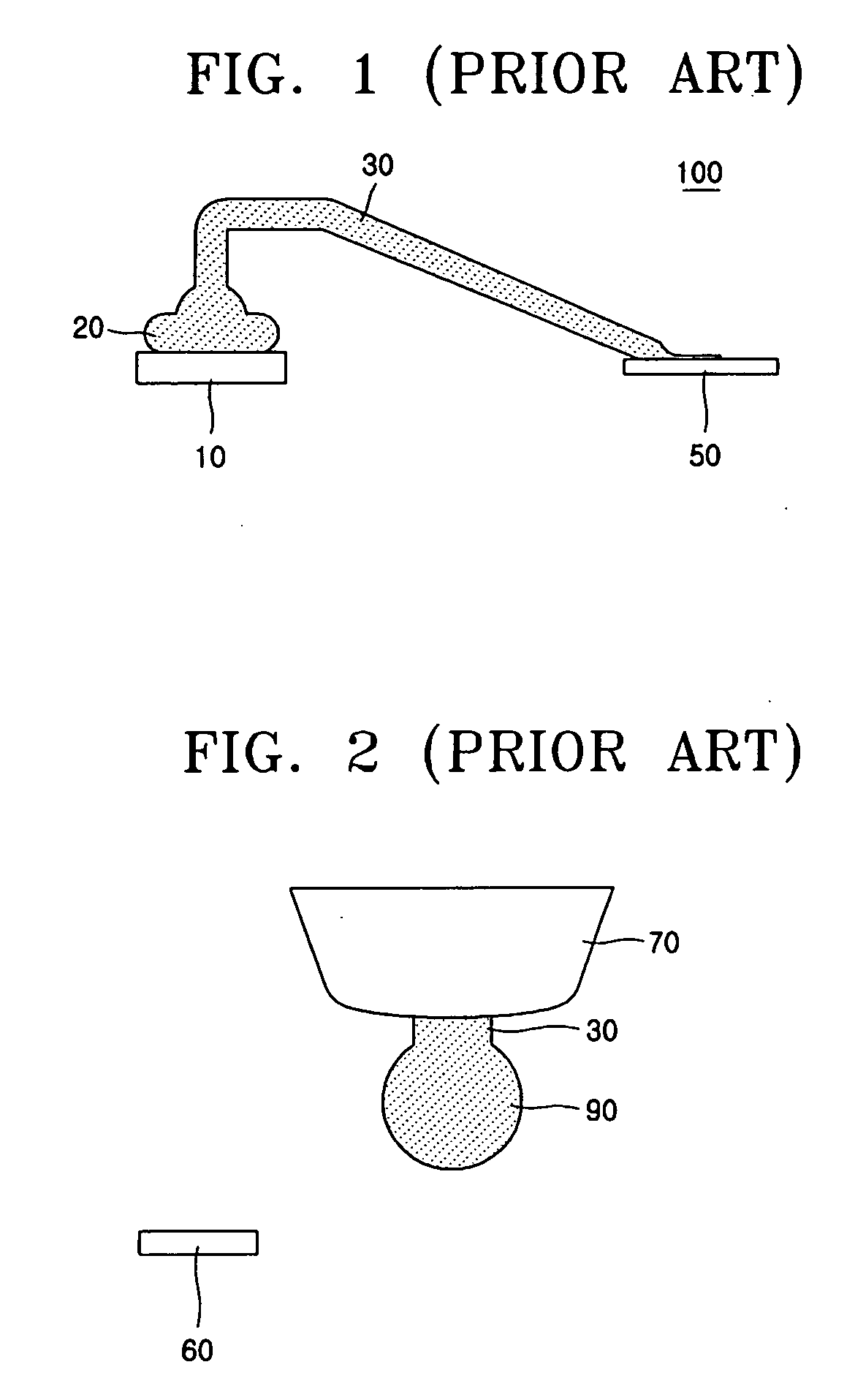
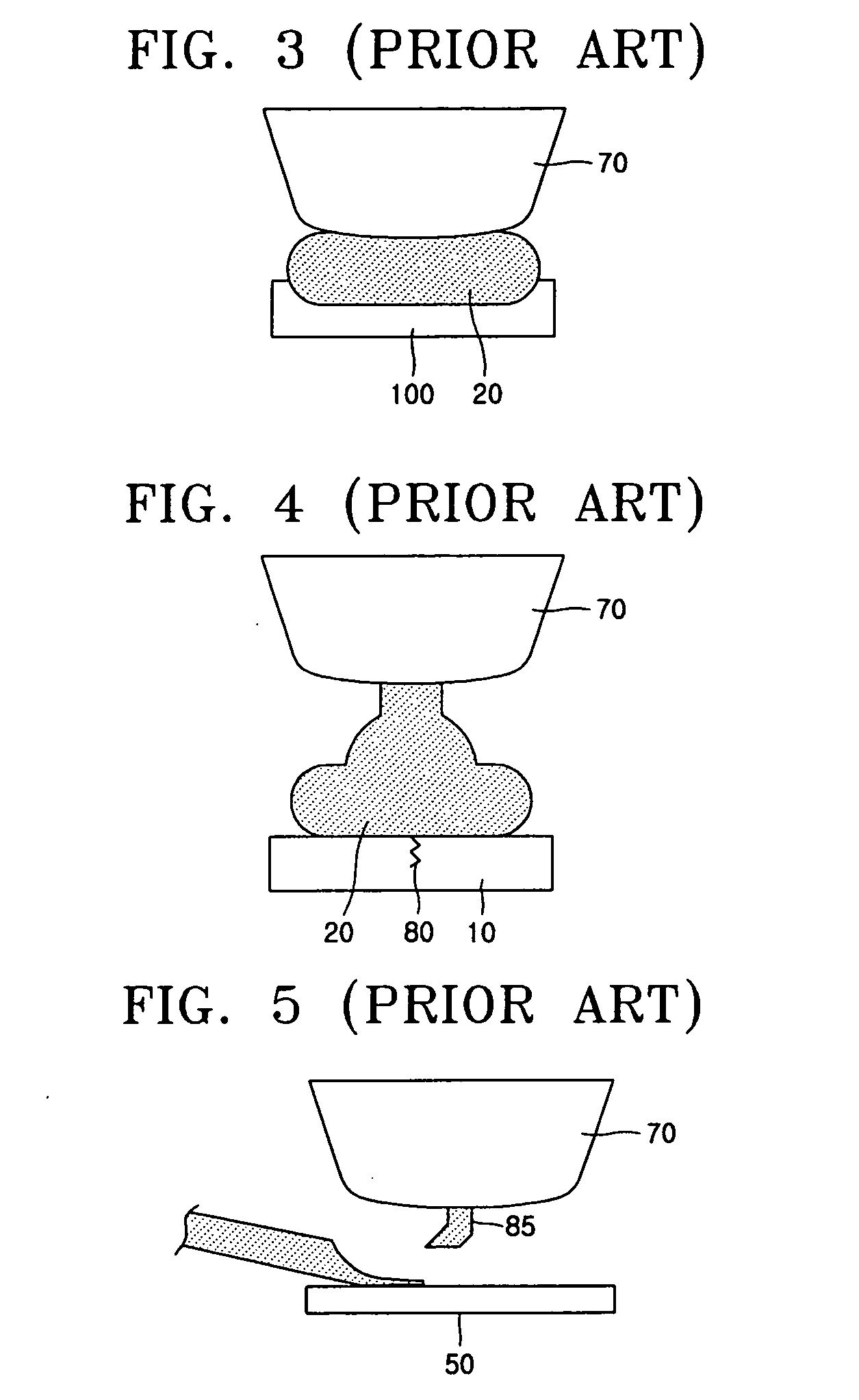
[0027] A copper bonding wire according to the present invention may be mainly formed of a high purity oxygen free copper including a small amount of impurities and not including oxygen. The high purity oxygen free copper is mixed with another element in the unit of wt ppm within a range keeping a high electric conductivity state of the high purity oxygen free copper to lower a hardness of the high purity oxygen free copper. Next, the high purity oxygen free copper is manufactured as a bonding wire. Thus, metal squeeze out, chip cratering, and a short tail occurring during bonding of the bonding wire to a semiconductor package can be prevented. A content of the high purity oxygen free copper may be adjusted so that the copper bonding wire is as hard as a gold bonding wire. However, a total content of an added element is adjusted so that a residual amount of the copper bonding wir...


PUM


Abstract

Provided is a copper bonding wire formed of a high purity copper of 99.999% or more including at least one of P and Nb within a range between 20 wt ppm and 100 wt ppm and at least one of Zr, Sn, Be, Nd, Sc, Ga, Fr, and Ra within a range between 1 wt ppm and 100 wt ppm. Here, a total content of the added elements is restricted within a range between 20 wt ppm and 200 wt ppm, and a residual amount of the copper bonding wire is a high purity copper of 99.98% or more. As a result, metal squeeze out and chip cratering can be reduced in a general semiconductor chip and a low dielectric semiconductor chip. Also, a short tail of the copper bonding wire occurring during bonding of the copper bonding wire to a lead finger can be reduced.

Description

CROSS-REFERENCE TO RELATED PATENT APPLICATION [0001] This application claims the benefit of Korean Patent Application No. 10-2005-0013511, filed on Feb. 18, 2005, in the Korean Intellectual Property Office, the disclosure of which is incorporated herein in its entirety by reference. BACKGROUND OF THE INVENTION [0002] 1. Field of the Invention [0003] The present invention relates to a copper bonding wire for semiconductor packaging, and more particularly, to a copper bonding wire easily applied to a package using a lead frame of parts used as external connectors. [0004] 2. Description of the Related Art [0005] Referring to FIG. 1, a semiconductor package 100 includes a semiconductor chip 10 and a lead part of a lead frame, i.e., a lead finger 50. The semiconductor chip 10 is formed of an integrated circuit (IC) using a non-conductor such as silicon (Si) or germanium (Ge) as a thin substrate. The lead finger 50 is connected to the semiconductor chip 10 via a bonding wire 30 to directl...

Claims


Application Information

Patent Timeline
IPC IPC(8): H01L23/48
CPCH01L24/45H01L2224/45015H01L2224/45147H01L2224/48095H01L2224/48247H01L2224/48465H01L2224/78301H01L2924/01004H01L2924/01014H01L2924/01015H01L2924/01029H01L2924/0103H01L2924/01031H01L2924/0104H01L2924/0105H01L2924/01059H01L2924/01061H01L2924/01064H01L2924/01073H01L2924/01075H01L2924/01077H01L2924/01079H01L2924/01082H01L2924/01088H01L2924/01203H01L2924/01205H01L2924/20755H01L2924/30105H01L2924/0106H01L2924/01087H01L2924/01021H01L2924/00014H01L2924/01019H01L2924/01033H01L2924/01041H01L2924/01055H01L2924/01076H01L2924/01084H01L2924/00H01L2924/013H01L24/43H01L2224/43848H01L2224/45144H01L2924/10252H01L2924/10253H01L2924/14H01L2924/00015H01L2924/01062H01L2924/01071H01L2924/01085A01G13/0237A01G13/10A01G2013/006B65D85/34B65D85/52
Inventor WON, SUNG-JOONKWON, OH MINLEE, SUNG MUN
Owner MK ELECTRON
Why Eureka
Try Eureka