Single event effect (SEE) tolerant circuit design strategy for SOI type technology

a technology of single event effect and circuit design, applied in the field of integrated circuits, can solve the problems of large area penalty, limited choice of very advanced technologies, and inability to handle submicron soi cmos

Inactive Publication Date: 2006-08-24
IOTA TECH
View PDF21 Cites 25 Cited by
  • Summary
  • Abstract
  • Description
  • Claims
  • Application Information

AI Technical Summary

Benefits of technology

[0009] The invention provides a solution to the above and other problems by replacing each of the Single Event Effect (SEE) susceptible transistors with a plurality of serially connected gates to ensure undisturbed output levels free of unwanted glitches or Single Event Transient (SET) and Single Event Upset (SEU).

Problems solved by technology

Most Single Event Effect (SEE) problems for Silicon On Insulator (SOI) type CMOS integrated circuits are caused by the momentarily forward biasing of the back-channel bipolar transistor of an OFF transistor.
However, most very deep submicron SOI CMOS can only handle a power supply at 1.8 v or lower.
Thus, using a high power supply can greatly limit the choices of very advanced technologies.
A large area penalty is required to provide enough capacitance and resistance in a conventional integrated circuit to improve the SEU resistivity.
Further, the additional RC delays impact the performance of the specific circuit directly.
In addition, it is time consuming for circuit and layout designers to come up with enough capacitance without costing too much silicon area to suppress glitches coming from SET for a regular CMOS or CMOS SOI process.

Method used


Image

  • Single event effect (SEE) tolerant circuit design strategy for SOI type technology
  • Single event effect (SEE) tolerant circuit design strategy for SOI type technology
  • Single event effect (SEE) tolerant circuit design strategy for SOI type technology

Examples


Embodiment Construction

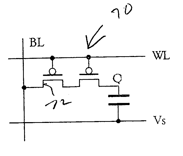
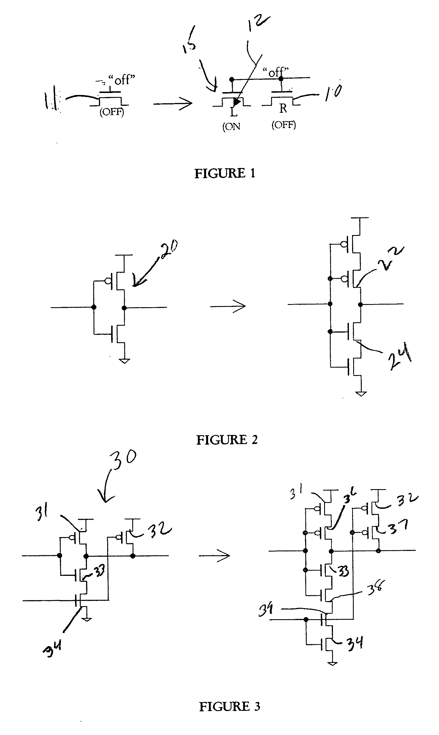
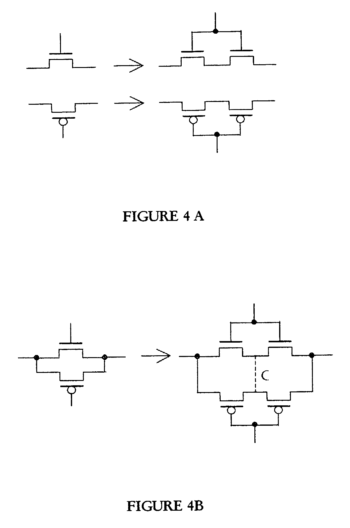
[0032] As indicated in FIG. 1, when a high-energy subatomic particle 12 strikes an integrated circuit with PN junctions, whole-electron pairs are produced. The state or drive characteristic of the circuit node connected to the struck PN junction can be altered or affected. For technologies like the SOI, SOA (Silicon-On-Anything), SOS, Bulk on Epi, or Bulk with buried oxide, where SEE can trigger the bipolar back-channel to turn on, an originally “OFF” transistor can be turned “ON” momentarily by the high-energy particle. For a driven node, the effect comes as a glitch if the strength of the driving transistor is not strong enough to overcome the momentarily turned “ON” of the bipolar back channel. This is called a Single Event Transient (SET). If the SET is allowed to propagate to a storage node and be latched, the original stored data is destroyed, which is called a Single Event Upset (SEU). The driving node can be an output of an inverter, buffer, passgate, NMOS, PMOS, tri-state d...


PUM


Abstract

A method of designing an integrated circuit to be Single Event Upset (SEU) immune by converting one or more Single Event Transient (SET) sensitive transistors into at least two serially connected transistors, and spacing the transistors sufficiently far apart so that the probability of a specified high-energy particle striking both transistors at the same time is remote.

Description

CROSS-REFERENCE TO RELATED APPLICATIONS [0001] This Application is a Non-Provisional Application of Provisional (35 USC 119(e)) Application No. 60 / 650,787 filed on Feb. 8, 2005 and claims the benefit thereof.FIELD OF THE INVENTION [0002] The invention relates to the field of integrated circuits, and more particularly, but not by way of limitation, to silicon-on-insulator (SOI) technology. BACKGROUND OF THE INVENTION [0003] As indicated in FIG. 1, when a high-energy subatomic particle 12 strikes an integrated circuit with PN junctions, whole-electron pairs are produced. The state or drive characteristic of the circuit node connected to the struck PN junction can be altered or affected. For technologies like the SOI, SOA (Silicon-On-Anything), SOS, Bulk on Epi, or Bulk with buried oxide, where Single Event Effect (SEE) can trigger the bipolar back-channel to turn on, an originally “OFF” transistor can be turned “ON” momentarily by the high-energy particle. For a driven node, the effec...

Claims


Application Information

Patent Timeline
Patent Type & Authority Applications(United States)
IPC IPC(8): G11C11/22
CPCG11C7/02G11C11/22G11C11/405G11C11/4125G11C2211/4016
Inventor HO, IU-MENG TOM
Owner IOTA TECH
Why Eureka
Try Eureka