Method for monitoring implantation depth of impurity

a technology of impurity implantation and depth, which is applied in the direction of individual semiconductor device testing, semiconductor/solid-state device testing/measurement, instruments, etc., can solve the problem that the implantation depth of the impurity b>70/b> cannot be monitored satisfactorily so far, and the present method is not capable of accurately detecting the variation in the implantation depth of the impurity, etc. problem, to achieve the effect of enhancing the efficiency of semiconductor device manufacturing

Inactive Publication Date: 2006-08-24
LAPIS SEMICON CO LTD
View PDF5 Cites 9 Cited by
  • Summary
  • Abstract
  • Description
  • Claims
  • Application Information

AI Technical Summary

Benefits of technology

[0049] Thus, the present invention is capable of accurately detecting a variation in the concentration peak depth Rp of the impurity as compared with the conventional method. Consequently, the variation in the concentration peak depth Rp of the impurity can be monitored satisfactorily.
[0050] Even when the injection energy E is relatively small in particular, the present invention is capable of satisfactorily monitoring a variation in impurity concentration peak depth Rp.
[0051] Incidentally, the wafer prepared for exclusive use has been utilized as the measuring wafer upon measurement of the implantation depth Rp of the impurity in the prior art. Therefore, there was conventionally a need to stop the production line in order to introduce the measuring wafer onto the production line

Problems solved by technology

However, when the ion implantation device continues to operate for a long period, it might implant an impurity to a depth different from the set value.
Such a phenomenon principally takes place due to the fact that malfunctions occur in each part of the ion implantation device.
Incidentally, an unillustrated device other than the ion implantation device may be caused to perform the heat treatment and the removal of the oxide film 14.
However, a variation in the implantation depth of the impurity 70 cou

Method used


Image

  • Method for monitoring implantation depth of impurity
  • Method for monitoring implantation depth of impurity
  • Method for monitoring implantation depth of impurity

Examples


first preferred embodiment

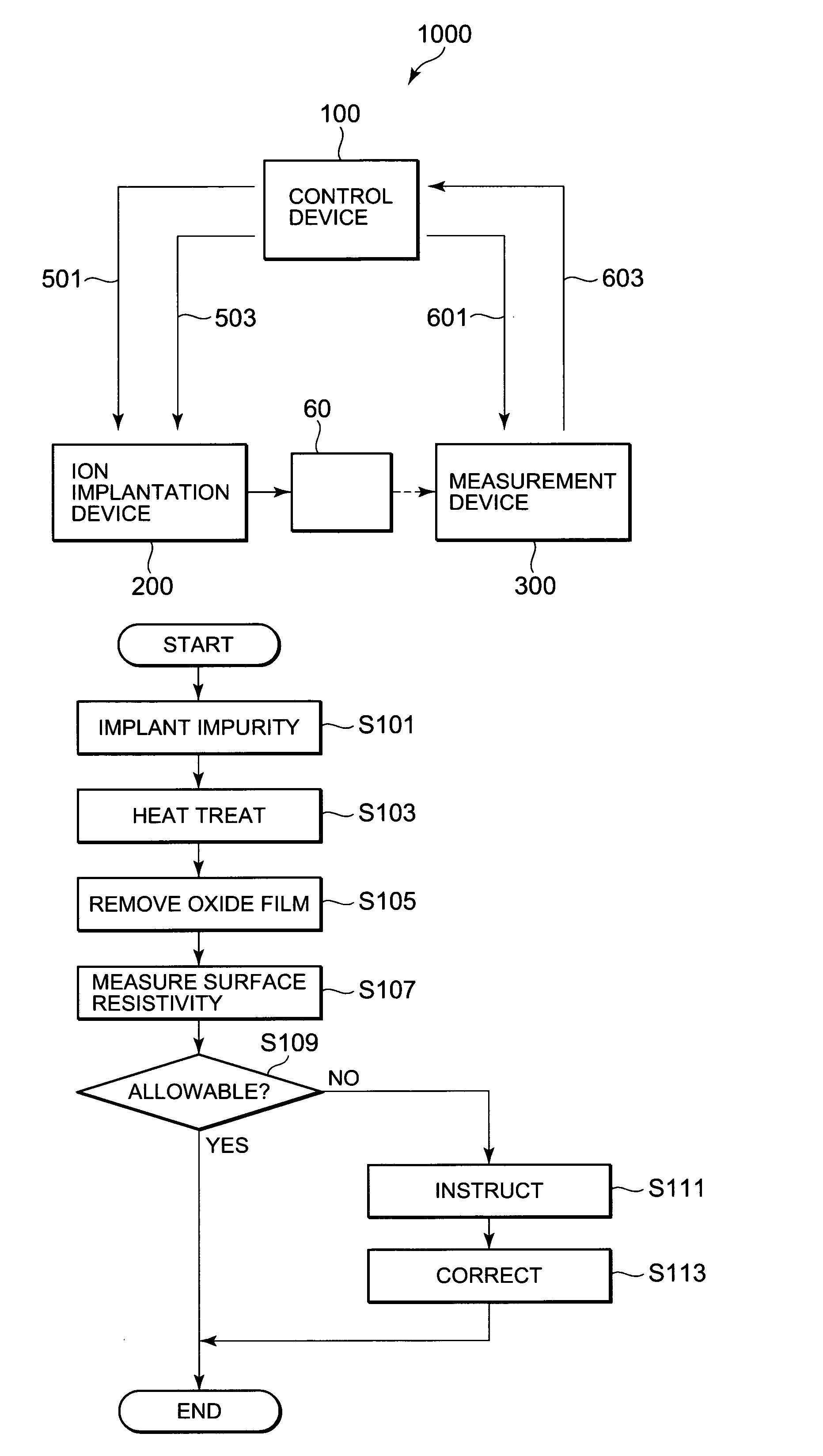
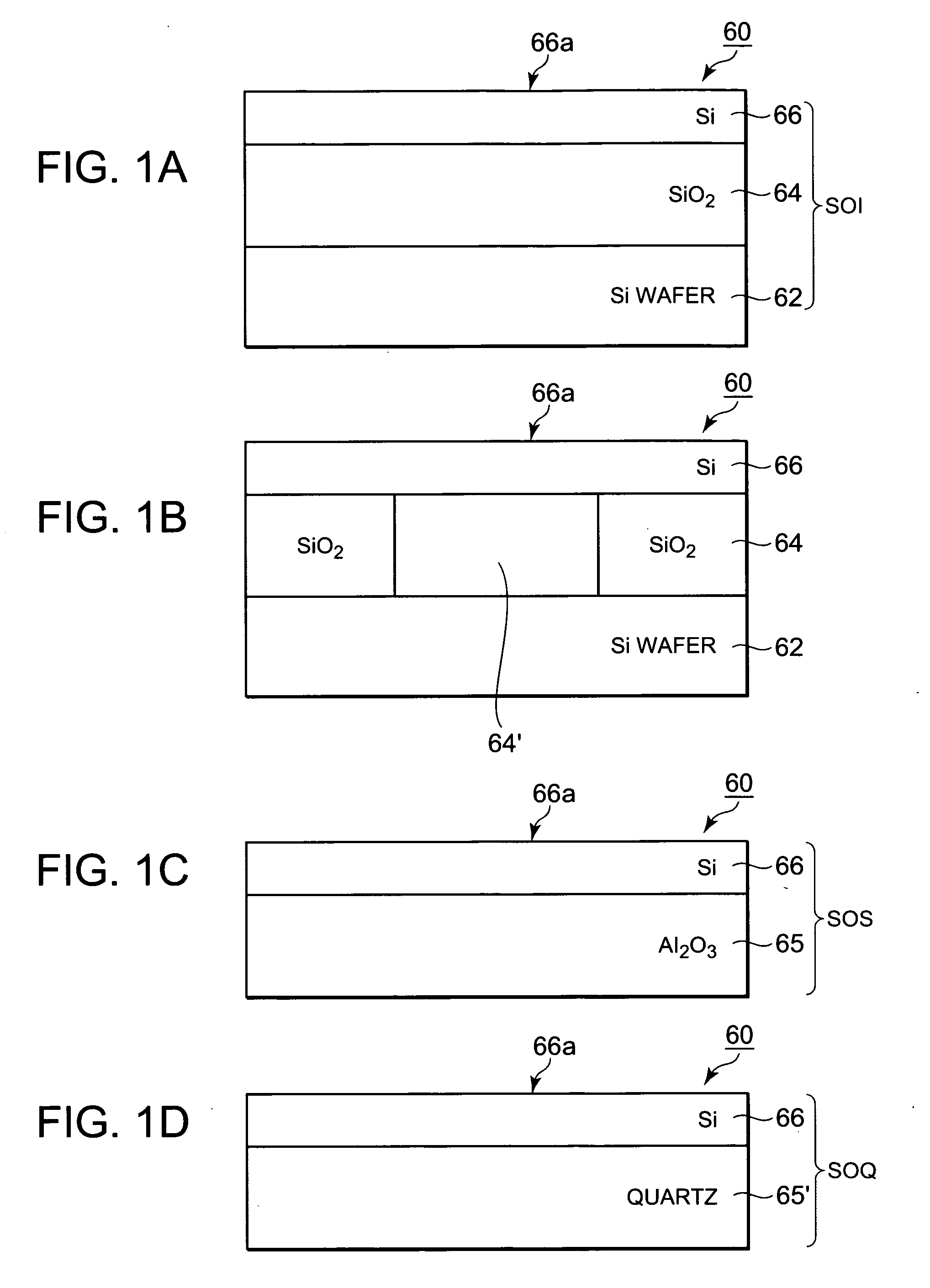
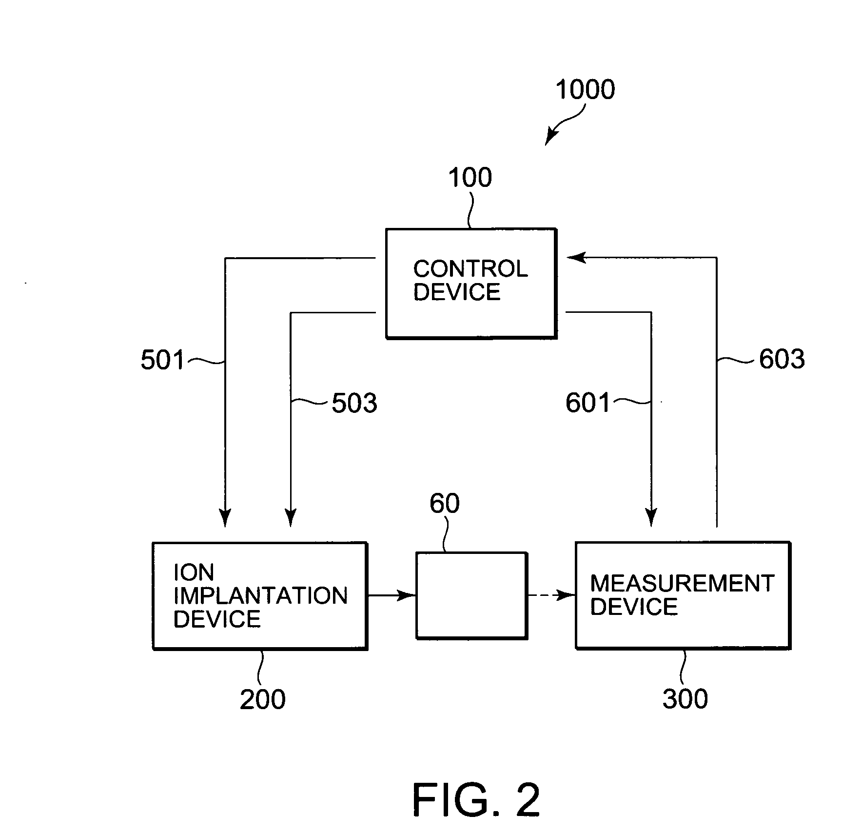
[0114] Respective preferred embodiments of the present invention will be explained below. In the respective embodiments, an SOI wafer is used as a measuring wafer 60, and phosphorus (P) is used as an impurity 70.

[0115]FIG. 7 is a view for describing a processing process according to a first embodiment. In order to explain the measuring wafer 60 employed in the first embodiment and the conventionally used measuring wafer 10 by comparison in FIG. 7, the measuring wafer employed in the first embodiment is referred to as “SOI wafer 60”, and the conventionally used measuring wafer is referred to as “bulk Si wafer 10”.

[0116] The first embodiment will be explained below with reference to FIG. 7A. The ion implantation device 200 first accelerates the impurity 70 at injection energy E set such that the impurity 70 is implanted to a set value RP of an implantation depth and injects the impurity 70 into the SOI wafer 60 from above a second oxide film 68. Incidentally, the injection energy E ...

second preferred embodiment

[0126]FIG. 8 is a view for describing a processing process according to a second embodiment. In the second embodiment, injection energy E is set higher than the first embodiment. Correspondingly, the thickness of a second oxide film 68 is formed thicker than the first embodiment. Incidentally, the thickness of the second oxide film 68 is set to such a thickness as not only to suppress outward diffusion of an impurity 70 but also to enable cutting of a base area of a concentration profile of the impurity 70.

[0127] The second embodiment will be explained below with reference to FIG. 8A. The ion implantation device 200 first accelerates the impurity 70 at injection energy E set such that the impurity 70 is implanted to a set value RP of its implantation depth and implants the impurity 70 in its corresponding SOI wafer 60 from above a second oxide film 68. Incidentally, the injection energy E is set in consideration of the thickness of the second oxide film 68 formed on its correspondi...

third preferred embodiment

[0136]FIG. 9 is a view for describing a processing process according to a third embodiment. In the third embodiment, a TEG pattern (Test Element Group pattern) for measuring a concentration peak depth Rp of an impurity 70 is formed on an SOI wafer 60 with the impurity 70 injected therein.

[0137]FIG. 9A shows the SOI wafer 60 subsequent to being subjected to the process (i.e., the oxide film removing process of S105) described with reference to FIGS. 7C and 8C.

[0138] The ion implantation device 200 effects photolithography processing and etching processing on an SOI layer 66 to form a TEG pattern 82. Thus, the ion implantation device 200 forms the TEG pattern 82 on a main surface of the SOI wafer 60 by using the SOI layer 66 (see FIG. 9B).

[0139] Next, the ion implantation device 200 forms an interlayer insulating film 84 and thereafter forms contacts 86 and wirings 88 on the TEG pattern 82. Thus, the TEG pattern 82 is made electrically conductive to the wirings 88 (see FIG. 9C).

[0...


PUM


Abstract

The present invention provides a method for measuring an implantation depth of an impurity injected into a wafer by an ion implantation device, using a measurement device and monitoring whether the measured implantation depth of impurity falls within an allowable range, comprising the steps of using, as a measuring wafer, a wafer having an insulating film and an Si layer formed on the insulating film with a thickness of a 1000 Å unit or less; implanting the impurity in the measuring wafer from above the surface of the Si layer, corresponding to a main surface of the measuring wafer and heat-treating the measuring wafer; and measuring surface resistivity of the main surface of the heat-treated measuring wafer by the measurement device and detecting, as an implantation depth of the impurity from the main surface, a concentration peak depth from the main surface, which corresponds to the surface resistivity and at which a concentration of the impurity implanted in the measuring wafer reaches a peak.

Description

BACKGROUND OF THE INVENTION [0001] 1. Field of the Invention [0002] The present invention relates to a method for satisfactorily monitoring the depth of an impurity implanted in a wafer upon manufacture of a semiconductor device. [0003] 2. Description of the Related Art [0004] Upon manufacture of a semiconductor device, an ion implantation device (not shown), which implants ion species (hereinafter called simply “impurity”) of impurities such as phosphorus (P), Arsenic (As), Boron, etc., needs to implant an impurity to a depth, which is given at a distance measured from a main surface of the wafer on the execution side of ion implantation and which is as expressed in a predetermined set value. [0005] However, when the ion implantation device continues to operate for a long period, it might implant an impurity to a depth different from the set value. Such a phenomenon principally takes place due to the fact that malfunctions occur in each part of the ion implantation device. Particul...

Claims


Application Information

Patent Timeline
IPC IPC(8): H01L21/66G01R31/26
CPCG01R31/2648H01L22/14
Inventor KISHIRO, KOICHI
Owner LAPIS SEMICON CO LTD
Why Eureka
Try Eureka