

Method for heat treatment of silicon wafers
a technology of heat treatment and silicon wafers, which is applied in the direction of semiconductor/solid-state device manufacturing, basic electric elements, electric devices, etc., can solve the problems that the inside of the wafer cannot be provided with the gettering capacity, and the defect-free wafer high in oxygen concentration cannot be applied as the device substra
Inactive Publication Date: 2006-08-24
SUMCO CORP
View PDF15 Cites 29 Cited by
- Summary
- Abstract
- Description
- Claims
- Application Information
AI Technical Summary
Benefits of technology
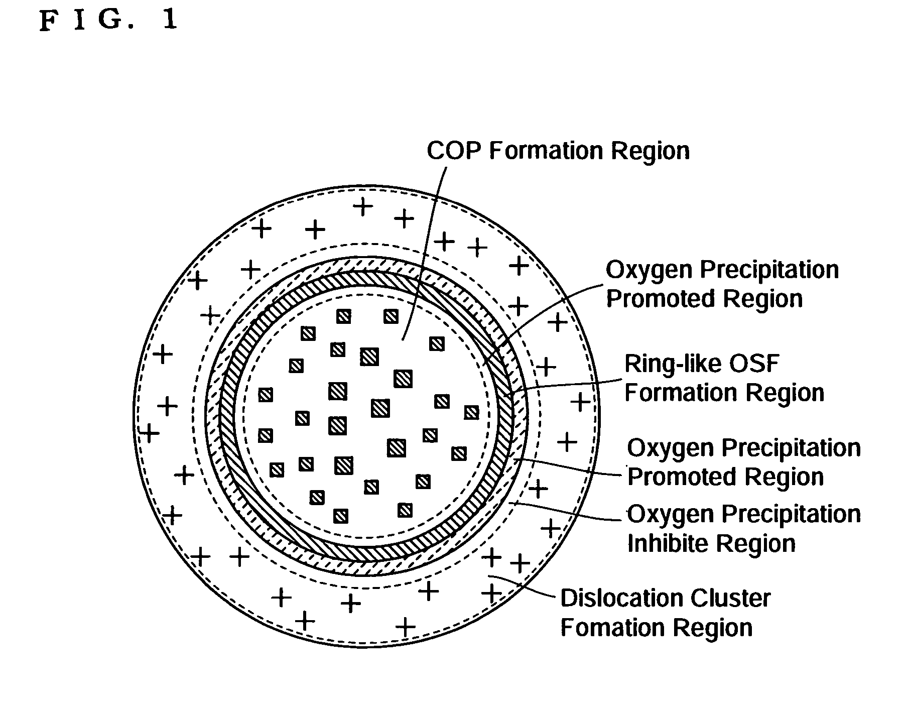
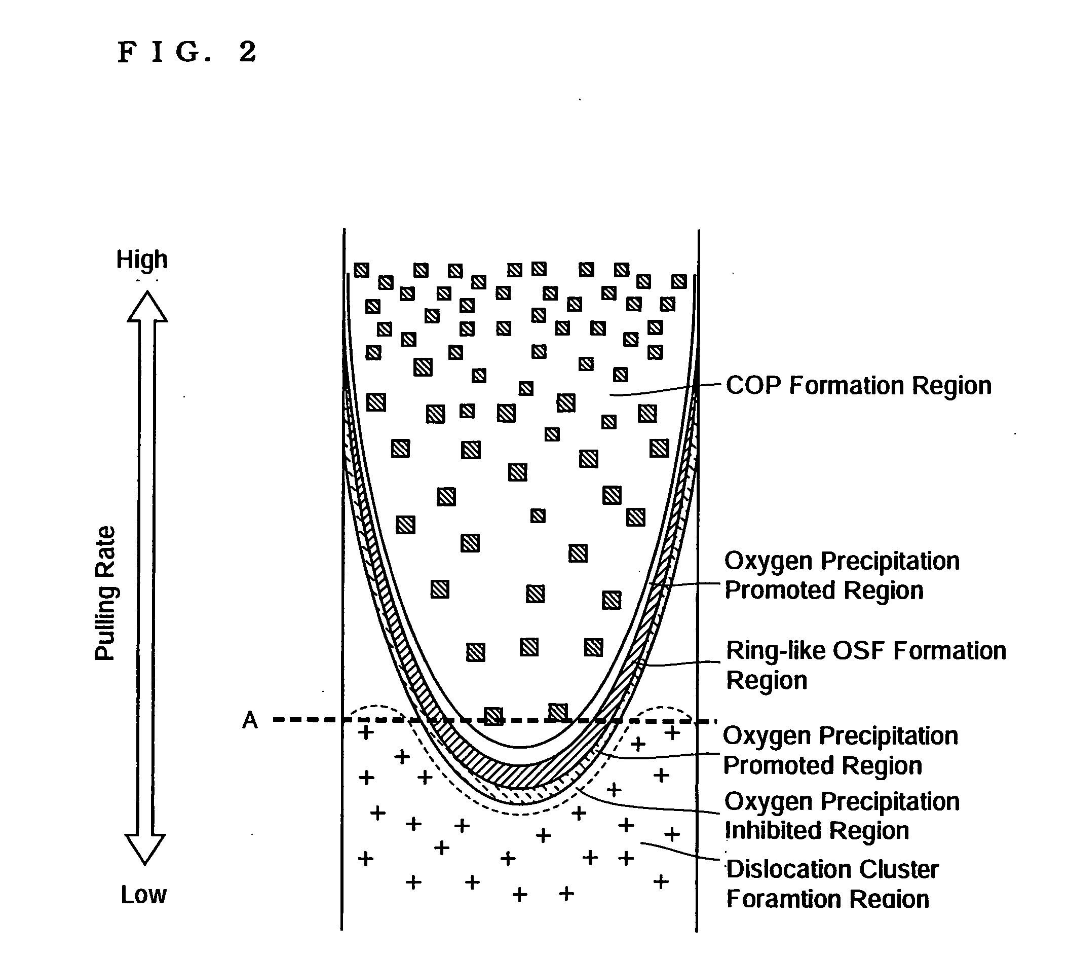
The present invention provides a method for heat treatment of silicon wafers that can improve the gettering capacity and stability of defect-free wafers. By subjecting wafers with a low oxygen concentration to high-temperature heat treatment in an oxygen atmosphere, the method can form a high oxygen concentration region under the surface of the wafer and promote the formation of oxygen precipitates. The method can also involve an oxidation heat treatment and an oxide precipitation heat treatment to further enhance the gettering capacity. The heat treatment method can be carried out using a rapid thermal annealing heater in a nitrogen gas-containing atmosphere to form vacancies and promote the formation of oxygen precipitates. The method can also involve a two-step heat treatment process to form stable oxygen precipitates. Overall, the heat treatment method can improve the quality of defect-free wafers and enhance the gettering effect.
Problems solved by technology
Therefore, the defect-free wafer high in oxygen concentration as such cannot be applied as the device substrate.
Therefore, with a wafer having an initial oxygen concentration lower than the above level, no oxygen precipitate can be formed, hence the inside of a wafer cannot be provided with the gettering capacity.
Method used
View moreImage
Smart ImageViewing Examples

Examples
examples
[0063] The effects of the silicon wafer heat treatment method by the present invention are described referring to certain specific examples, namely Comparative Examples 1 and 2, and Inventive Examples 1 to 5 which are embodiments of the present invention.
Login to View More PUM
| Property | Measurement | Unit |
|---|---|---|
| temperature | aaaaa | aaaaa |
| temperature | aaaaa | aaaaa |
| temperature | aaaaa | aaaaa |
Abstract
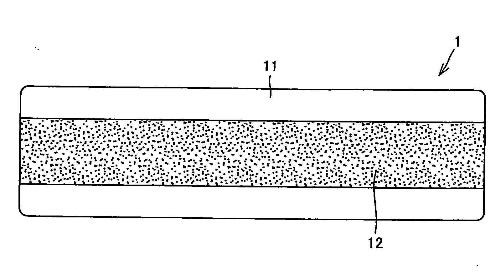
A method is provided for the heat treatment of low oxygen concentration silicon wafers obtained from a silicon single crystal produced by the Czochralski process. The method comprises high-temperature oxidation heat treatment for the formation of a high oxygen concentration region under the wafer surface and the subsequent oxygen precipitation heat treatment. The high-temperature oxidation heat treatment can cause inward diffusion of oxygen from the wafer surface to form a region increased in oxygen concentration under the wafer surface, and the subsequent oxygen precipitation heat treatment can form a DZ layer on the wafer surface and stably form oxygen precipitates optimal in size within the wafer at a high density, so that excellent gettering effects can be produced. Further, in case of using as SOI substrates formed by SIMOX, too, the same effects as mentioned above can be produced by carrying out the high-temperature oxidation heat treatment after oxygen ion implantation in the SIMOX process and then carrying out the oxygen precipitation heat treatment.
Description
BACKGROUND OF THE INVENTION [0001] 1. Field of the Invention [0002] This invention relates to a method for heat treatment of silicon wafers having a low oxygen concentration and, more particularly, to a method for heat treatment of silicon wafers wherein a silicon wafer having a low oxygen concentration and having a defect-free region all over the whole surface thereof is subjected to oxidation heat treatment at high temperature for formation of a high oxygen concentration region in the vicinity of the surface and the subsequent oxygen precipitation heat treatment, whereby a defect-free layer (denuded zone (DZ) layer) can be formed on the wafer surface and oxide precipitate (bulk micro defect (BMD)) formation within the wafer can be promoted. [0003] 2. Description of the Related Art [0004] In recent years, the levels of quality requirements imposed on silicon single crystals produced by the Czochralski process (hereinafter, “CZ process”) serving as device substrates have been increa...
Claims
Login to View More Application Information
Patent Timeline
 Patent Type & AuthorityApplications(United States)
IPC IPC(8): H01L21/324
CPCH01L21/3225H01L21/324
InventorADACHI, NAOSHIKOMATSU, YUKIO
OwnerSUMCO CORP