Methods of manufacturing electrical contacts having solder stops

a technology of solder stop and electrical contact, which is applied in the manufacture of contact parts, manufacturing tools, laser beam welding apparatus, etc., can solve the problems of reduced electrical performance of electrical connection between, reduced integrity of mechanical connection between electrical contact and printed circuit board, and reduced solder amount, so as to prevent solder wicking and prevent solder wicking. , the effect of preventing the wicking of solder

Inactive Publication Date: 2006-09-07
SAMTEC
View PDF42 Cites 18 Cited by
  • Summary
  • Abstract
  • Description
  • Claims
  • Application Information

AI Technical Summary

Benefits of technology

[0006] Several techniques are known in the art to prevent solder wicking, and more specifically, to prevent solder from wicking up along the length of the contact body of an electrical connector. First, it is known to use a nickel barrier to prevent solder wicking. Nickel is known as a solder anti-wicking material. A typical electrical contact is formed by coating or plating a base layer of copper or copper alloy with a nickel layer. The nickel layer is then coated or plated with an additional layer of tin, gold, or silver.
[0007] In order to use the nickel layer as an anti-wicking layer, selective plating, belt masking, spot plating, and controlled depth plating are typically required. In selective plating, the additional layer must be selectively plated such that a portion of the nickel layer is left exposed. This is accomplished by using removable mask materials such that a portion of the nickel layer is covered when the additional layer is plated. After the additional layer is plated, the removable mask materials are removed, along with the additional layer, such that the nickel layer is exposed.
[0...

Problems solved by technology

The reduction in the amount of solder has the following disadvantageous effects: (a) causes a reduction in the electrical performance of the electrical connection between the electrical contact and the printed circuit board; (b) causes a reduction in the integrity of the mechanical connection between the electrical contact and the printed circuit board; (c) hinders mating of the electrical contact with the printed circuit board; and (d) reduces the aesthetics of the completed mechanical connection.
A problem with these techniques is that it is hard to accurately plate the additional layer such that nickel layer is exposed in a location that is most effective for preventing the wicking of the solder.
This problem increases the cost of production of any contact that uses the above-described techniques.
An additional problem with these techniques is that exposed nickel is not a very effective anti-wicking material.
Thus, the flux reduces the effectiveness of the oxidized nickel as an anti-wicking material.
A problem with this technique is that the hole in the contact acts to degrade any electrical signal traveling through the contact and to degrade the mechanical strength of the contact.
Another problem with this technique is the cost of the secondary process of punching a hole during manufacturing of the contact.
A proble...

Method used


Image

  • Methods of manufacturing electrical contacts having solder stops
  • Methods of manufacturing electrical contacts having solder stops
  • Methods of manufacturing electrical contacts having solder stops

Examples


Embodiment Construction

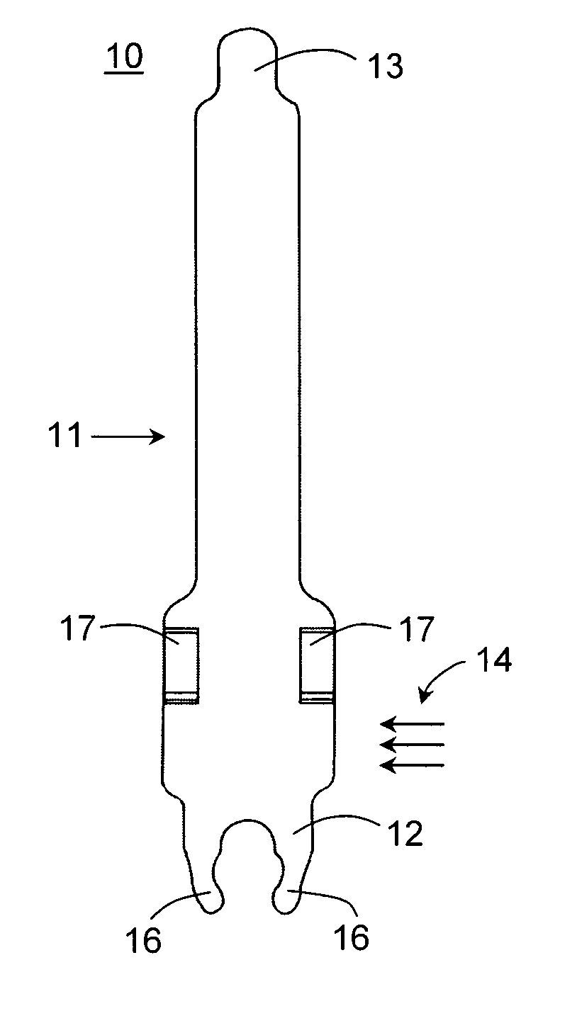
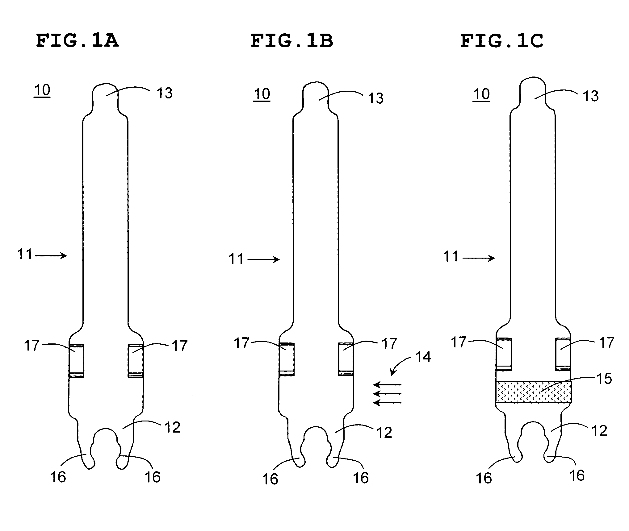
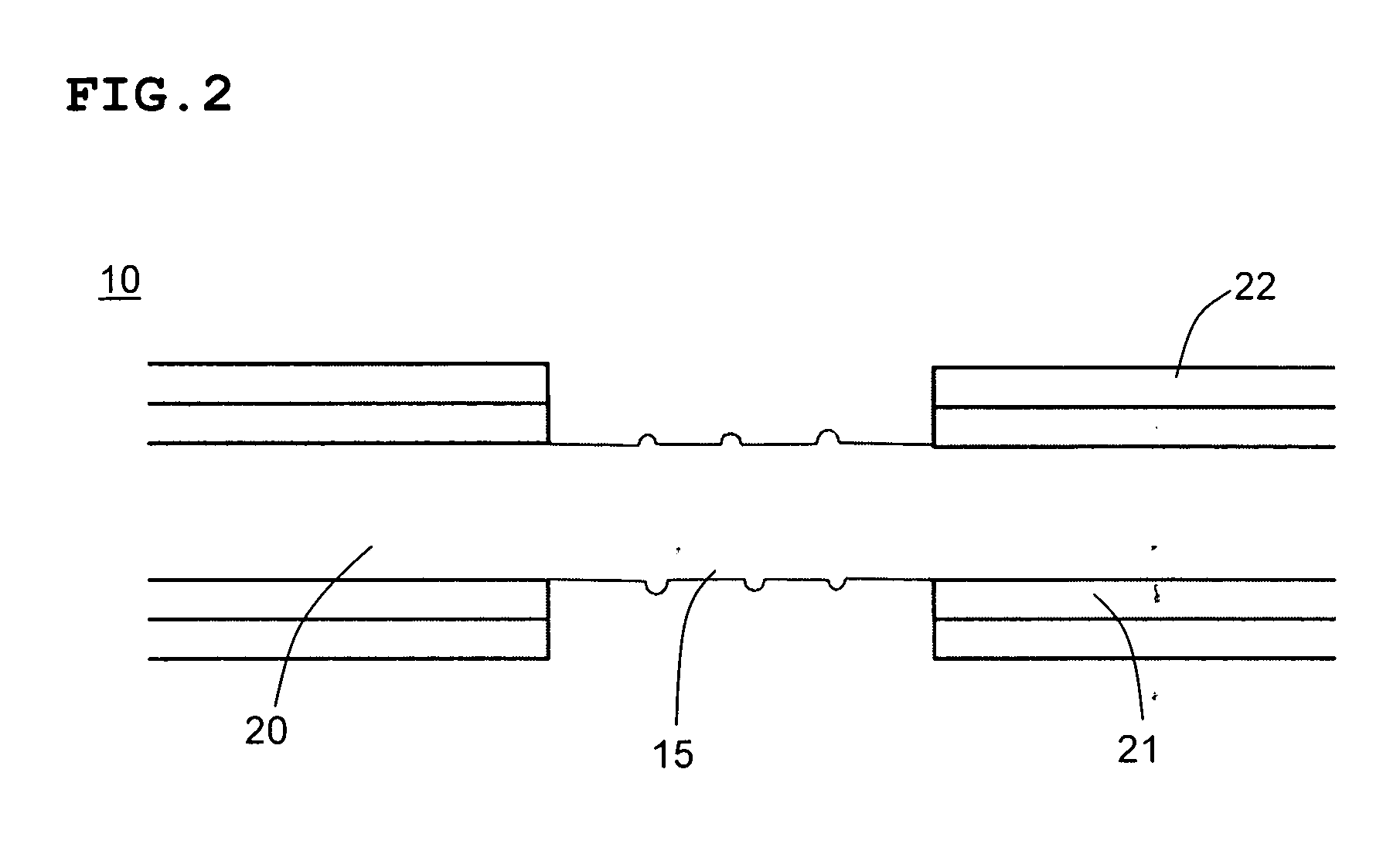
[0053]FIGS. 1A-1C illustrate a method of manufacturing, according to a first preferred embodiment of the present invention, an electrical contact 10 according to a second preferred embodiment of the present invention. FIG. 2 illustrates a close-up sectional view of an anti-wicking region 15 of the electrical contact 10.

[0054]FIG. 1A illustrates the electrical contact 10 having a contact body 11. The contact body 11 includes a contact tail 12 and a contact head 13. As shown in FIG. 1A, the contact tail 12 includes arms 16 for holding a fusible material, such as solder or a solder member (not shown). However, other arrangements for attaching solder to the contact tail 12 could also be used for attaching the fusible material in the form of, for example, solder balls or solder charges. Further, the contact tail 12 need not include any arrangement for holding solder. Instead, the fusible material or solder could be provided on any substrate to which the electrical contact 10 is to be so...


PUM

PropertyMeasurementUnit
Temperatureaaaaaaaaaa
Electrical resistanceaaaaaaaaaa

Abstract

A method of forming an electrical contact for use in an electrical connector that includes a contact body made of metal and having a contact head, a contact tail, and an anti-wicking region disposed between the contact head and the contact tail arranged to prevent wicking of a fusible material past the anti-wicking region in a direction toward the contact head. The anti-wicking region is defined by one of a laser-ablated portion, a laser marking material, a UV marking material, and an ink that is permanently disposed on the contact body.

Description

BACKGROUND OF THE INVENTION [0001] 1. Field of the Invention [0002] The present invention relates to solder stops. More specifically, the present invention relates to solder stops on electrical contacts and to methods of making electrical contacts having solder stops. [0003] 2. Description of the Related Art [0004] As shown in FIG. 6, it is well known in the art to use solder 64 to form an electrical connection between a connection pad 65 on a printed circuit board 66 and the contact tail 63 of an electrical contact 60. When the solder 64 is reflowed to join the contact tail 63 of the electrical contact 60 to the connection pad 65 on the printed circuit board 66, the solder 64 will wick up the length of the contact body 61, which reduces the amount of solder 64 located between the contact tail 63 of the electrical contact 60 and connection pad 65 on the printed circuit board 66. [0005] The reduction in the amount of solder has the following disadvantageous effects: (a) causes a redu...

Claims


Application Information

Patent Timeline
IPC IPC(8): B23K26/36
CPCH01R4/028H01R43/16
Inventor VICICH, BRIANKOOPMAN, STEVE
Owner SAMTEC
Why Eureka
Try Eureka