

Non-volatile memory and manufacturing method and operating method thereof
a manufacturing method and non-volatile memory technology, applied in the field of memory devices, can solve the problems of difficult to increase the level of integration of non-volatile memory, and cannot be used as multi-level memory cell devices, so as to improve device performance and increase the level of integration of memory cells
- Summary
- Abstract
- Description
- Claims
- Application Information
AI Technical Summary
Benefits of technology
Problems solved by technology
Method used
Image

Examples
Embodiment Construction
[0036] Reference will now be made in detail to the present embodiments of the invention, examples of which are illustrated in the accompanying drawings. Wherever possible, the same reference numbers are used in the drawings and the description to refer to the same or like parts.
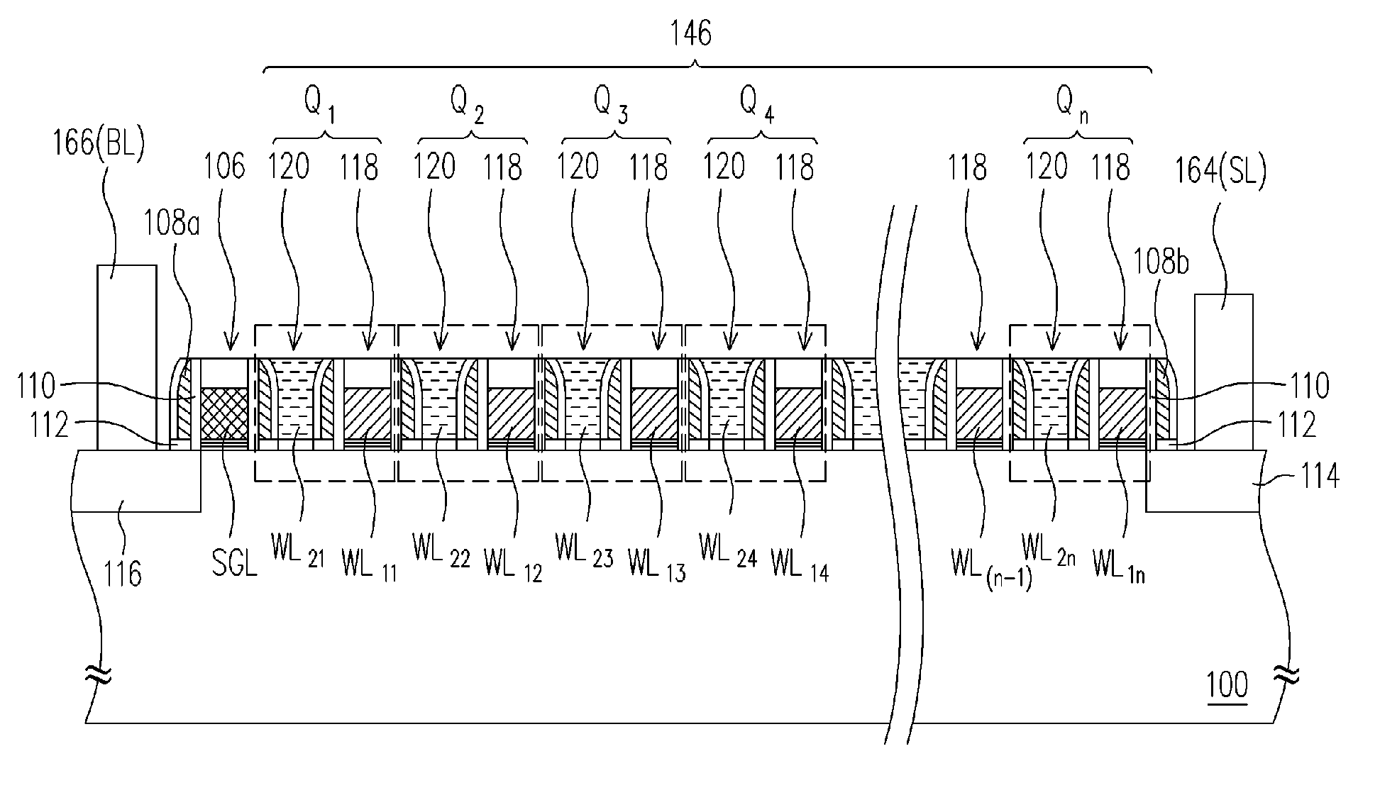
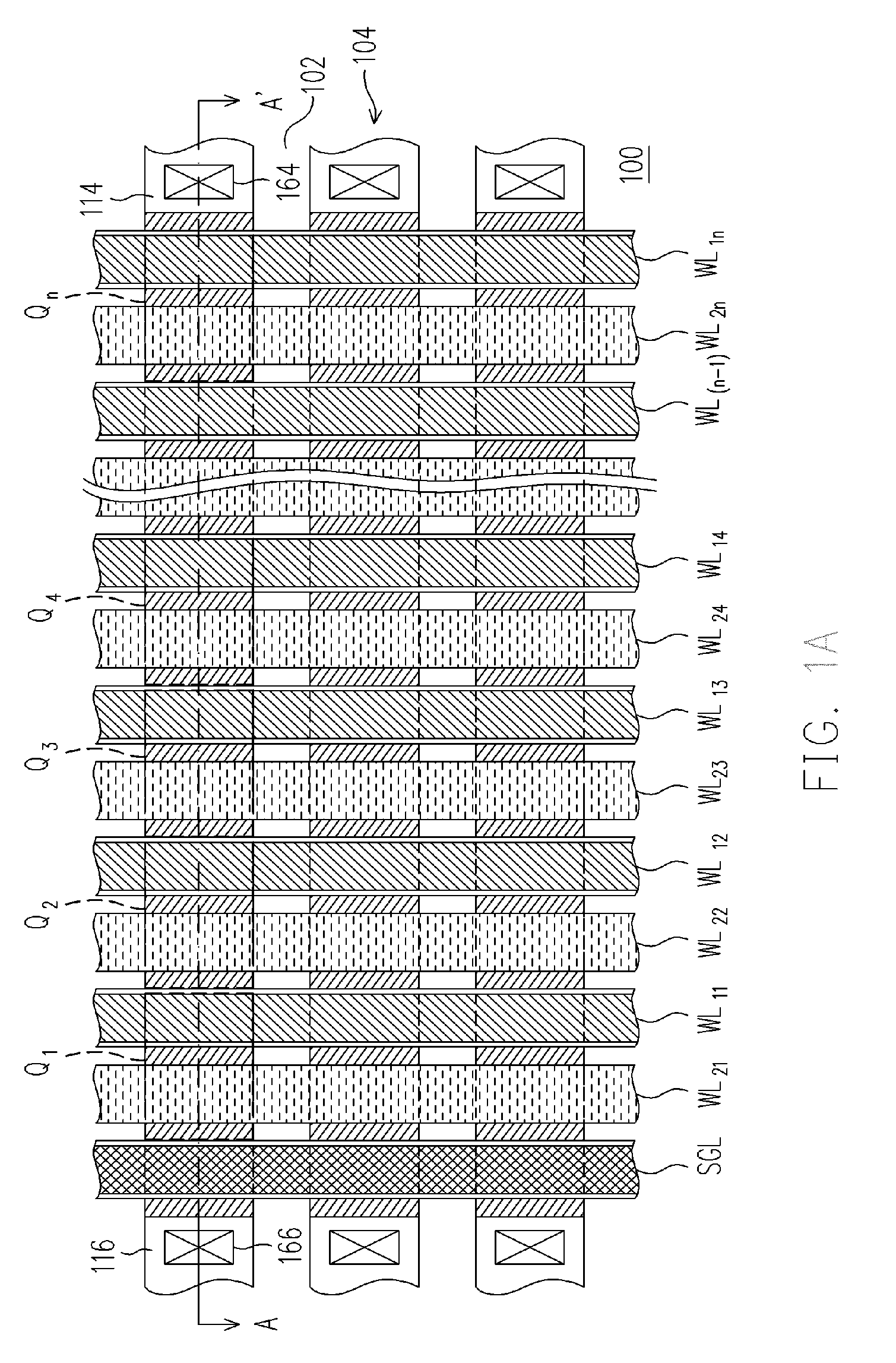
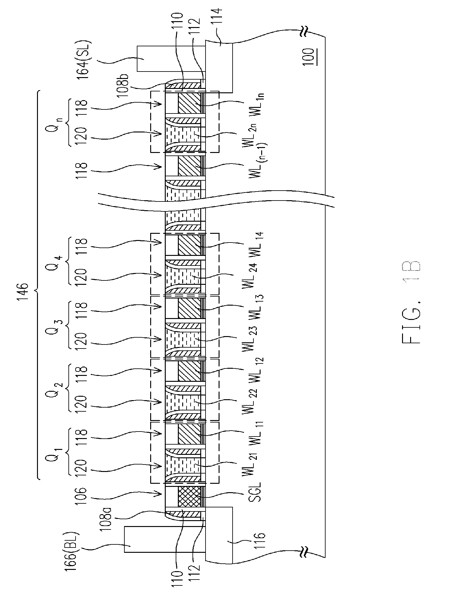
[0037]FIG. 1A is a top view showing a non-volatile memory according to the present invention. FIG. 1B is a schematic cross-sectional view along line A-A′ of FIG. 1A. FIG. 1C is a schematic cross-sectional view of the structures of a memory cell and a select unit according to the present invention. As shown in FIGS. 1A, 1B and 1C, the non-volatile memory of the present invention at least includes a substrate 100, a device isolation structure 102, an active region 104, a plurality of memory units Q1˜Qn, a select unit 106, a plurality of conductive spacers 108a, 108b, an insulating layer 110, a gate dielectric layer 112, a source region 114 and a drain region 116.
[0038] The substrate 100 is a silicon substrate...
PUM
 Abstract
Description
Claims
Application Information