Method and system for defect detection

Inactive Publication Date: 2006-09-07
ONTO INNOVATION INC
View PDF9 Cites 38 Cited by
  • Summary
  • Abstract
  • Description
  • Claims
  • Application Information

AI Technical Summary

Benefits of technology

[0013] To overcome the deficiencies in the prior art described above, the present invention provides an improved design for an optical inspection system. The present invention provides an improved design for maximizing sensitivity in defect detection while statistically increasing robustness. In one aspect, the present invention is a method for inspecting an object, and specifically a structure-bearing surface of an object, by scanning the object with an optical platform having one or more light sources for illuminating the object's surface and a camera for capturing one or more images of the illuminated object. The method also includes determining which of a number of available defect detection sche

Problems solved by technology

These structures are often so small that they can barely be seen, if at all, with the naked eye.
And ultimately, finished products require inspection so that defective ones are not used.
Existing systems are far from perfect, however.
For example, all optical imaging systems are limited in resolution by fundamental optical principles related to the wavelength of light, numerical aperture of the apparatus used, and by the overall geometry of the system.
In addi

Method used


Image

  • Method and system for defect detection
  • Method and system for defect detection
  • Method and system for defect detection

Examples


Embodiment Construction

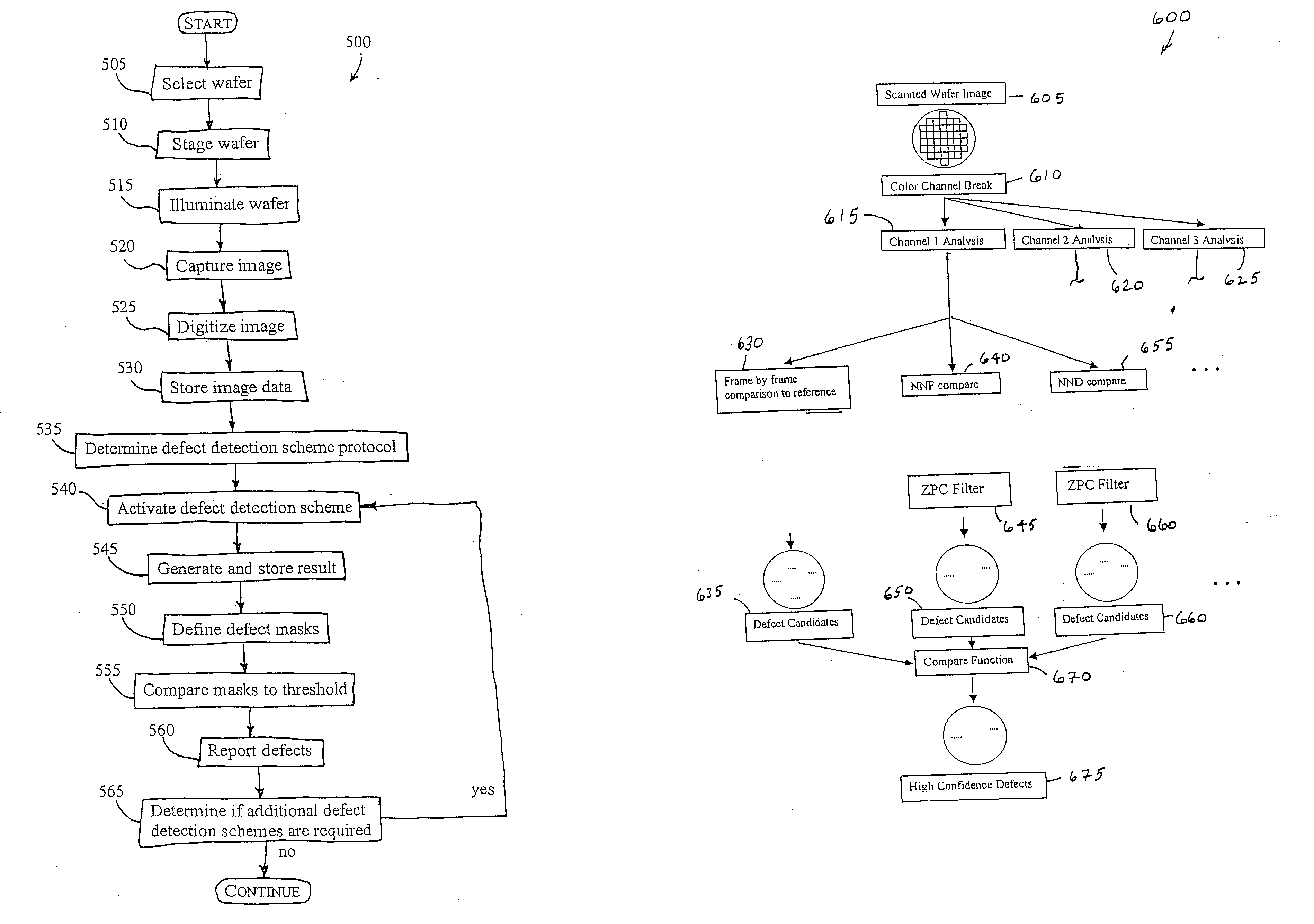
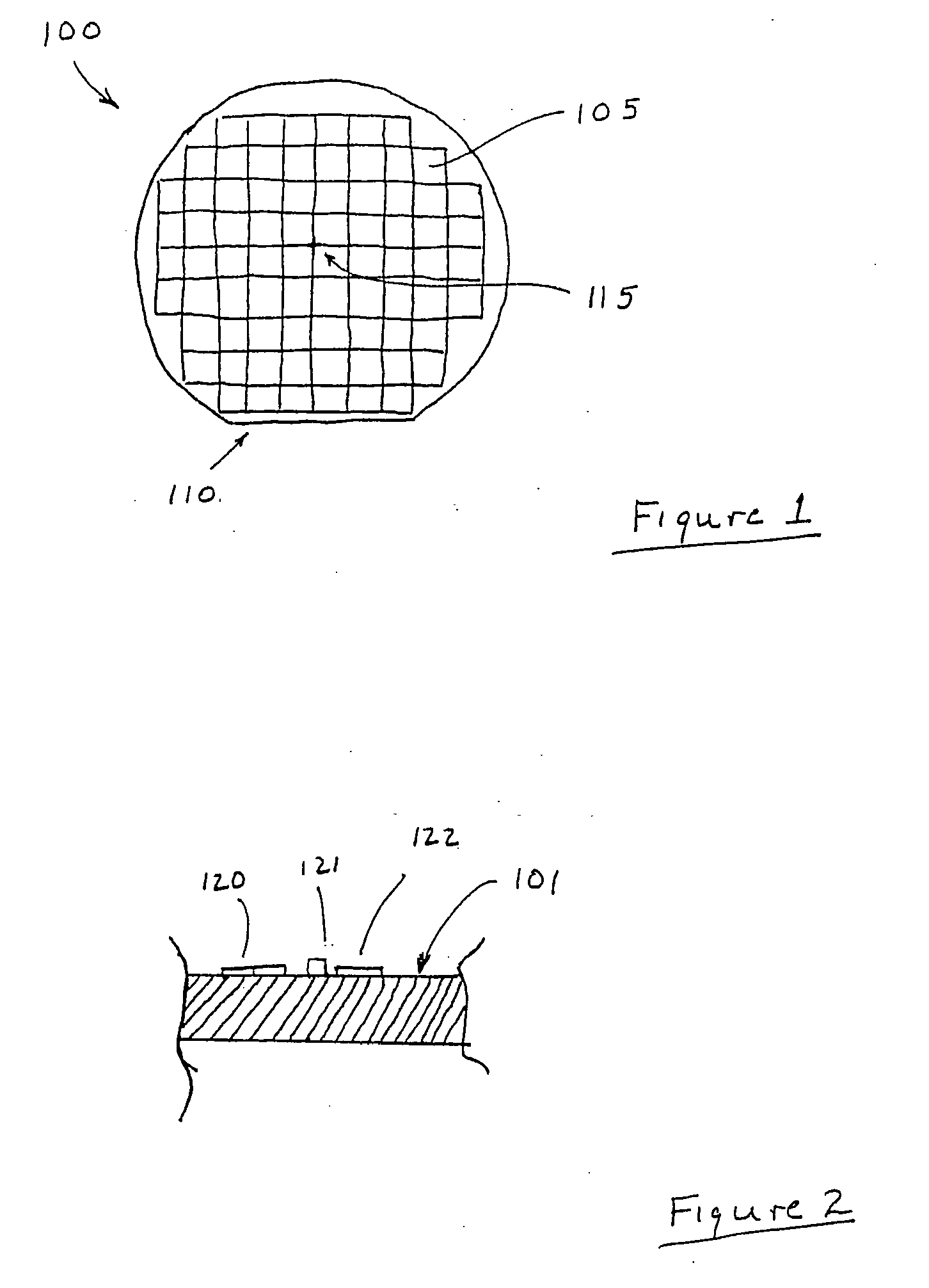
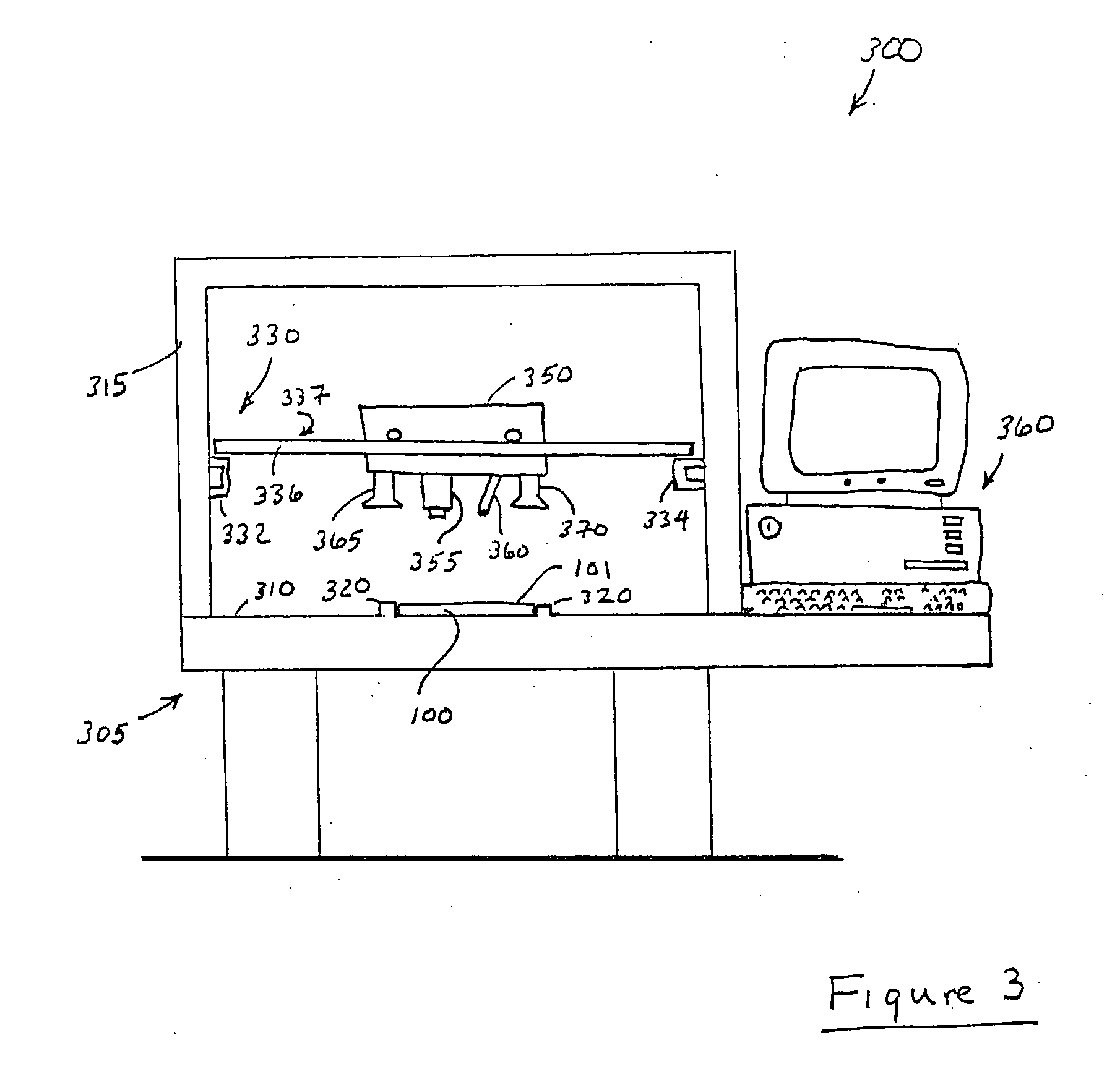
[0024] The present invention is directed to a method and system for performing inspections using an optical platform for collecting images of an object and then processing the images in a manner that produces a higher degree of confidence that the defects involving features formed on its surface, if any, have been properly identified. The present invention exploits multiple independent detection schemes and correlates them using a defect mask to increase detection sensitivity while decreasing unwanted nuisance defects. The method and system of the present invention are especially advantageous when applied to the inspection of semiconductor wafers and printed circuit boards during the production process.

[0025] The present invention will now be described in such an embodiment, that is, one useful for inspecting semiconductor wafers during the manufacturing process. The method and system of the present invention may, for example, be used to inspect wafers to which photoresist has been...


PUM


Abstract

A method for inspecting objects such as semiconductor wafers. A staging platform and an optical platform are arranged so that the object may be staged and its surface scanned by optical equipment situated on the optical platform. During the scanning process, the surface is illuminated with light of a plurality of wavelengths, each strobed at a predetermined rate so that multiple images may be collected using time and frequency multiplexing. The multiple images are stored in a database for analysis, which includes processing selected ones of the multiple images according to one or more algorithms. The defect-detection algorithms used for each object are determined by referenced to a predetermined or calculated defect detection protocol, then a defect mask is created for each pixel in the images that is suspected to be defective. The defect mask is then compared to threshold parameters to determine which if any of the suspected defects should be reported.

Description

[0001] This application claims the benefit of U.S. Provisional Application No. 60 / 658,914 filed on 4 Mar. 2005, the disclosure of which is hereby incorporated by reference.TECHNICAL FIELD [0002] The present invention is directed generally to the field of defect detection, and more specifically to a method and system for inspecting objects such as semiconductor wafers or printed circuit boards to detect defects using an automated inspection system that yields a high degree of statistical confidence in the result, thus ensuring that as many defects as possible are discovered, and also that non-defective products are not erroneously identified for discard or repair. BACKGROUND [0003] There are many kinds of electrical and electronic devices that are widely available for scientific, business, and consumer-oriented applications. Rapid advances in technology have allowed their use to migrate from universities and large institutions to small businesses and homes. Computers are now popular,...

Claims


Application Information

Patent Timeline
IPC IPC(8): H01L21/66G01R31/26
CPCG01N21/9501
Inventor FU, YONGHANGLIU, YONGQIANGDARWIN, MICHAEL J.
Owner ONTO INNOVATION INC
Why Eureka
Try Eureka