Thin film semiconductor device and method of manufacturing a thin film semiconductor device

a thin film semiconductor and manufacturing method technology, applied in the direction of sustainable manufacturing/processing, final product manufacturing, basic electric elements, etc., can solve the problems of limiting the size of the semiconductor device, degrading according to the process, and high production cos

Active Publication Date: 2006-09-07
PST SENSORS
View PDF29 Cites 53 Cited by
  • Summary
  • Abstract
  • Description
  • Claims
  • Application Information

AI Technical Summary

Problems solved by technology

The first two are expensive to produce and are aimed at the high end of the market.
Consequently, all commercial photovoltaic semiconductor devices are over-engineered so that they degrade according to the specification and are consequently fitted with regulators to keep the output voltage constant.
In commercial semiconduction based solar cells, the substrate is typically glass which limits the size of the semiconductor device due to its mechanical stability and weight.
Glass also has the added disadvantage of being rigid and brittle.
A major factor limiting the production of inexpensive semiconductor devices, is the use of vacuum deposition processes in the production.
Such vacuum deposition processes are relatively expensive and as such, add significantly to the cost of producing semiconductor devices.
Further, semiconductor layers deposited using CVD processes are relatively rigid and as such, do not combine well with flexible substrates.

Method used


Image

  • Thin film semiconductor device and method of manufacturing a thin film semiconductor device
  • Thin film semiconductor device and method of manufacturing a thin film semiconductor device
  • Thin film semiconductor device and method of manufacturing a thin film semiconductor device

Examples


example 2

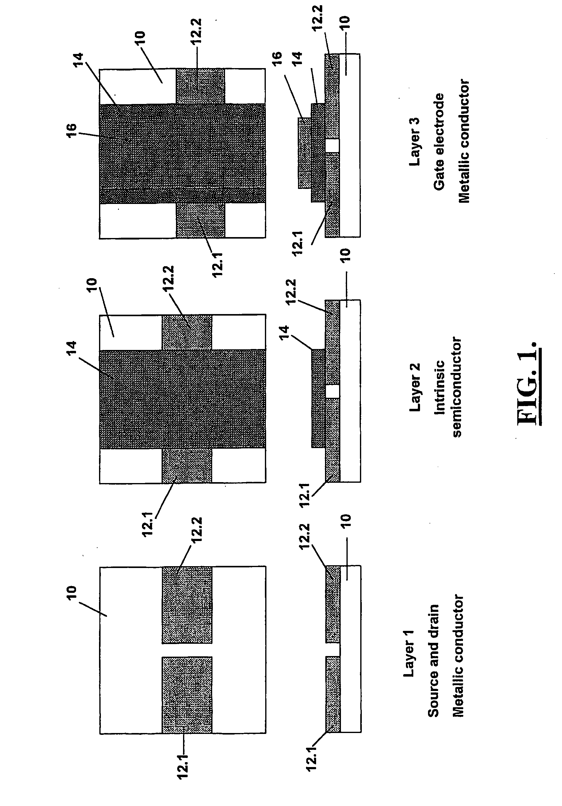
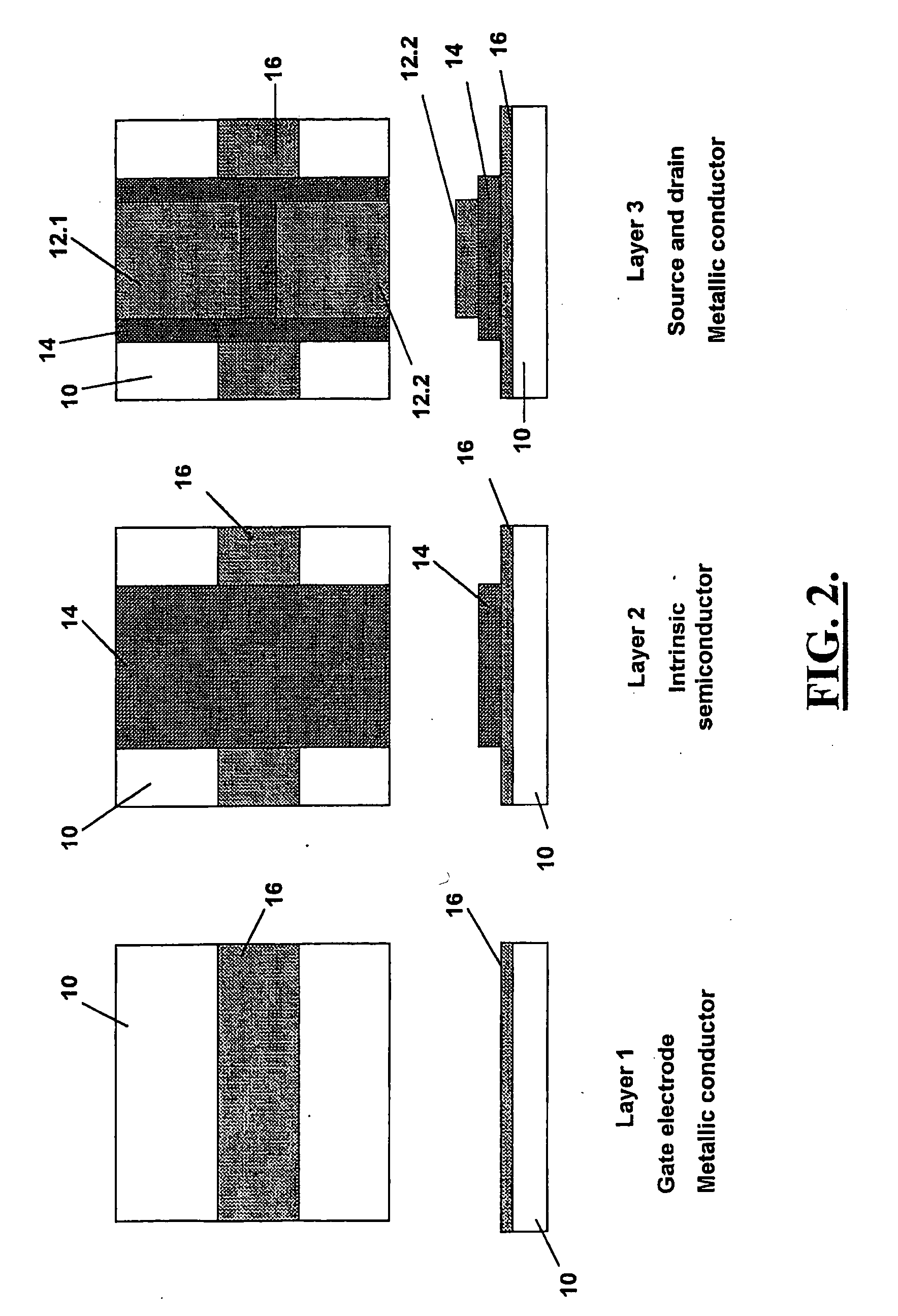
[0035]FIG. 2 shows a bottom gate MS-FET comprising three thin film semiconductor layers which are supported on a substrate 10 of paper sheet. The bottom gate MS-FET is the same as the top gate MS-FET illustrated in FIG. 1, with the only difference being that the semiconductor layers have been reversed to form a bottom gate field effect transistor. This allows direct connection of other active components to the source and drain of the transistor for faster switching. The same reference numerals are used in FIG. 2 to designate features of the bottom gate MS-FET that are the same as those of the top gate MS-FET shown in FIG. 1. In this example, the same printing process and material used in the top gate MS-FET of Example 1, is used for the various semiconductor layers.

[0036] With reference to FIG. 6 of the drawings, the current-voltage characteristics of a prototype bottom gate MS-FET manufactured by the Applicant in accordance with the invention, are illustrated. The prototype MS-FET...

example 3

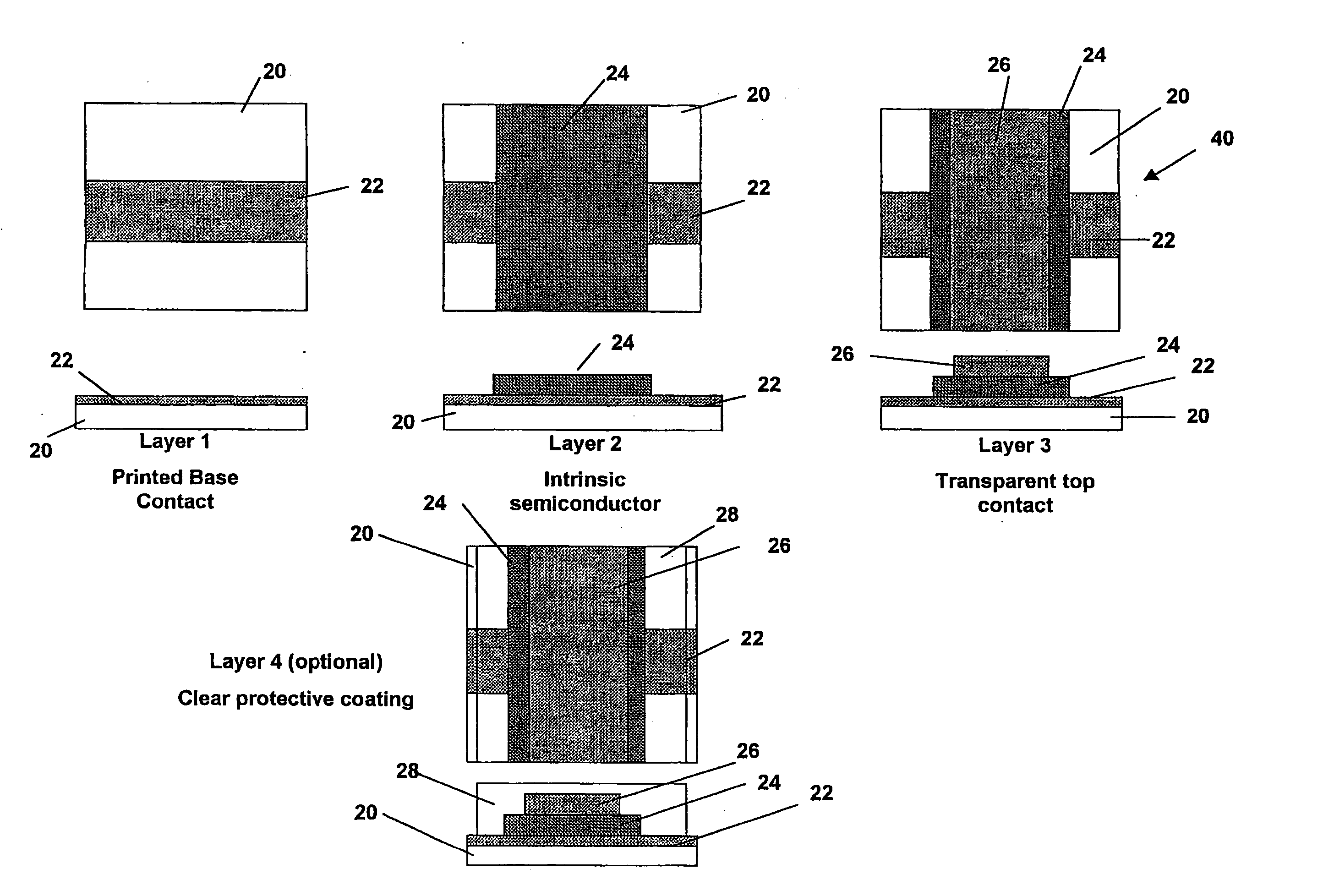
[0037] With reference to FIG. 3 of the drawings, a thin film semiconductor in the form of a photovoltaic cell 40 is shown which comprises an intrinsic semiconductor 24 (layer 2) sandwiched between two electrodes. More particularly, the photovoltaic cell comprises a first active layer in the form of a metallic base contact 22 of, for example, colloidal silver that is printed onto a major surface of a paper substrate 20 of plain white office paper such as Mondi Rotatrim wood free paper. The second active layer in the form an intrinsic semiconductor, is applied to the first layer. The second layer comprises, for example, colloidal nc-Si which is printed onto the first layer. A third active layer which forms a top contact is a transparent p-type conductor 26, for example, of colloidal indium tin oxide (ITO) such as Dupont Luxprint 7162E translucent conductor material, which is printed onto the second layer. The fourth layer which is optional, is in the form of a clear protective coating...

example 4

[0039] This example shows a construction of a photovoltaic battery which comprises three layers which are deposited onto a paper substrate 20. The battery comprises three photovoltaic cells 40 which are connected in series. The first layer is in the form of a printed metallic base contact 50, for example, of colloidal silver which is printed onto the paper substrate 10. The second layer comprises a single intrinsic semiconductor layer or a semiconductor structure in n-i-p sequence comprising, for example, a colloidal nc-Si layer that is printed onto the first layer. The photovoltaic battery includes a third layer comprising a transparent top contact 54 of, for example, colloidal ITO, that is printed onto the second layer. It will be appreciated that individual battery cells are laid down as strips across the paper substrate 10 by overlapping the top and bottom contacts of neighbouring strips, the cells are automatically connected together in series.

[0040] Only two external connecti...


PUM


Abstract

A thin film semiconductor in the form of a metal semiconductor field effect transistor, includes a substrate 10 of paper sheet material and a number of thin film active inorganic layers that are deposited in layers on the substrate. The active layers are printed using an offset lithography printing process. A first active layer comprises source 12.1 and drain 12.2 conductors of colloidal silver ink, that are printed directly onto the paper substrate. A second active layer is an intrinsic semiconductor layer 14 of colloidal nanocrystalline silicon ink which is printed onto the first layer. A third active layer comprises a metallic conductor 16 of colloidal silver which is printed onto the second layer to form a gate electrode. This invention extends to other thin film semiconductors such as photovoltaic cells and to a method of manufacturing semiconductors.

Description

FIELD OF INVENTION [0001] THIS INVENTION relates to a thin film semiconductor device. [0002] It also relates to a method of manufacturing a thin film semiconductor device. BACKGROUND OF INVENTION [0003] Semiconductor devices currently in production or under commercial development, can be classified in three categories: single crystalline silicon, bulk polycrystalline silicon or thin film semiconductor. The first two are expensive to produce and are aimed at the high end of the market. Most research and development is aimed at improving the efficiency and long-term stability of such devices with little regard to cost. [0004] On the other hand, thin film semiconductors are generally intended for lower cost applications, where absolute efficiency and compactness is not a prerequisite. Long-term stability is still a desirable goal for existing thin film semiconductors because of the relatively high production costs and the high material costs of the substrate. [0005] Most commercial thi...

Claims


Application Information

Patent Timeline
Patent Type & Authority Applications(United States)
IPC IPC(8): H01L21/84H01L23/02H01L21/20H01L21/208H01L21/336H01L29/49H01L31/0224H01L31/0392H01L31/20
CPCH01L31/022425H01L29/16H01L31/202Y02E10/50H01L31/046H01L21/02422H01L21/02488H01L21/02491H01L21/02521H01L21/02532H01L21/02601H01L21/02628Y10S977/775Y10S977/778Y10S977/785H01L29/66848H01L29/8126H01L31/03921Y02P70/50
Inventor HARTING, MARGITBRITTON, DAVID THOMAS
Owner PST SENSORS
Why Eureka
Try Eureka