Preparation method for crystalline silicon solar cell nanometer transparent buried gate electrode

A technology of solar cells and buried gate electrodes, applied in circuits, electrical components, semiconductor devices, etc., can solve the problems of anti-reverse carrier collection rate, nano transparent electrodes and silicon chip ohmic contact problems that have not been mentioned, and achieve Excellent carrier collection efficiency, low cost, and simple preparation method

Active Publication Date: 2013-03-20
SOUTH CHINA NORMAL UNIVERSITY
View PDF3 Cites 13 Cited by
  • Summary
  • Abstract
  • Description
  • Claims
  • Application Information

AI Technical Summary

Problems solved by technology

[0011] The inventor proposed a method for preparing a nano-transparent electrode on the surface of a silicon wafer with a pyramid structure in the method for preparing a transparent electrode for a crystalline silicon solar cell disclosed in the Chinese inv

Method used


Image

  • Preparation method for crystalline silicon solar cell nanometer transparent buried gate electrode
  • Preparation method for crystalline silicon solar cell nanometer transparent buried gate electrode
  • Preparation method for crystalline silicon solar cell nanometer transparent buried gate electrode

Examples


Embodiment Construction

[0056] The present invention will be described in detail below in conjunction with the embodiments and accompanying drawings.

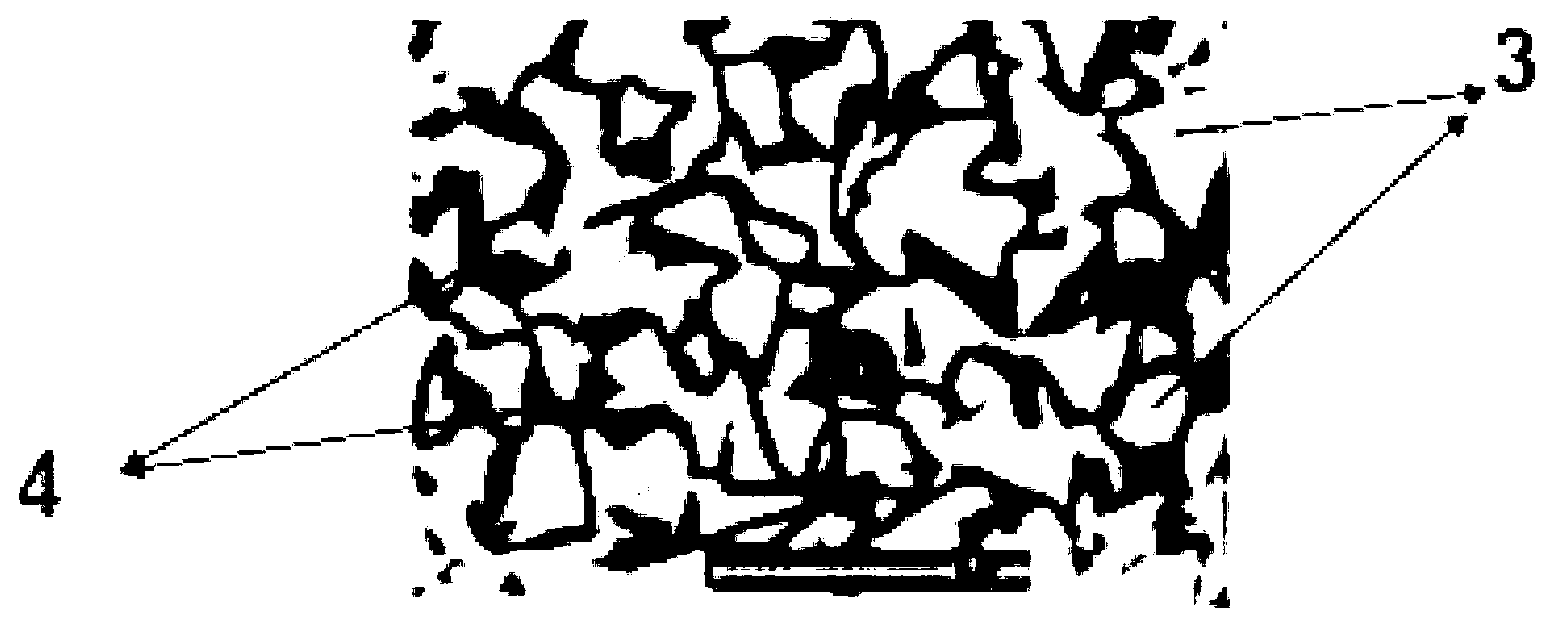
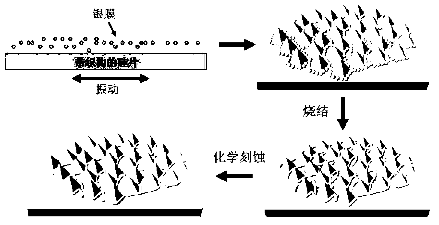
[0057] Such as image 3 The present invention discloses a method for preparing a nano-transparent buried gate electrode of a crystalline silicon solar cell, which includes four main steps: the first is the synthesis of silver ink solution, and the second is the agglomeration of nano-silver particles on the silicon surface with a pyramid texture The third is the sintering and annealing of metal nano-silver particle agglomerates to form interconnected metal nanowires / rod networks, and the fourth is metal-assisted chemical etching of samples to embed metal nanowires / rod networks into silicon wafers to form nano-buried gate transparent electrodes.

[0058] 1. Preparation of silver ink solution

[0059] Metallic silver nanoparticles used in electrodes can be synthesized by wet chemical methods. The invention adopts a simpler synthesis method, that is, a ...


PUM


Abstract

The invention relates to a preparation method for a crystalline silicon solar cell nanometer transparent buried gate electrode. The preparation of an electrode sample includes a first step of dripping silver ink solutions to the surface of a silicon wafer with a pyramid suede structure, exerting vibration in the horizontal direction on the silicon wafer, and enabling the whole surface of the silicon wafer to form an aggregate structure with evenly distributed nanometer silver particles, a second step of sintering the electrode sample, heating the electrode sample through microwave radiation and enabling the nanometer silver particles to be mutually fused to form mutually connected metal nanometer line or bar network structures, a third step of carrying out metal auxiliary chemical etching to the electrode sample, carrying out metal auxiliary etching process to the sample after being sintered in mixed solutions of hydrofluoric acid, hydrogen peroxide and ethanol, and enabling the metal nanometer line or bar network electrode to be inserted into the silicon wafer to form the nanometer transparent buried gate electrode. After the metal auxiliary chemical etching, antireflection effects of the metal nanometer line or bar networks inserting into the silicon wafer are remarkably optimized, contact resistance of the metal nanometer line or bar network electrode and the silicon wafer is remarkably decreased, and the electrode has a function of an antireflection layer and potential excellent carrier collection efficiency.

Description

technical field [0001] The invention belongs to the technical field of photovoltaic application and photoelectric application, and in particular relates to a method for preparing a nanometer transparent buried gate electrode of a crystalline silicon solar cell. Background technique [0002] As the storage of traditional energy such as oil and coal gradually decreases on the earth, green energy solar energy, as a substitute for traditional energy, has attracted more and more attention from the world. In solar energy applications, solar cells are key elements in photovoltaic technology that directly converts sunlight into electrical energy, and are widely used in various fields. [0003] The core structure of solar cells is the p-n junction. When sunlight with energy higher than the semiconductor band gap energy is incident on the p-n junction of the solar cell, electron-hole pairs are generated. Under the action of the self-built electric field on the p-n junction, electron...

Claims


Application Information

Patent Timeline
IPC IPC(8): H01L31/18H01L31/0224
CPCY02P70/50
Inventor 高进伟裴颗韩兵王洋
Owner SOUTH CHINA NORMAL UNIVERSITY
Why Eureka
Try Eureka