Integrated optics spot size converter and manufacturing method

a technology of spot size converter and integrated optics, applied in the field of optical components, can solve the problems of difficult reproducibility of specific spot size, difficult use in actual waveguide structures, and more complicated structures, and achieve the effect of improving the coupling of components and low loss

Active Publication Date: 2006-09-14
IGNIS PHOTONYX AS
View PDF12 Cites 61 Cited by
  • Summary
  • Abstract
  • Description
  • Claims
  • Application Information

AI Technical Summary

Benefits of technology

[0084] These steps provide the separation of the chip on which the optical component is included from the rest of the substrate (which preferably is a part of a wafer holding a number of (optionally) identical integrated optical circuits) (step g)) and improve the coupling of the component to an external waveguide, e.g. an optical fibre (step h)).
[0085] In an embodiment, the method in step d) further comprising the sub-step of d1) providing that the tapering of the core region of said first waveguide element of s

Problems solved by technology

However, as mentioned afore, this type of SSC is highly dependent upon the actual line width making it difficult to use in actual waveguide structures.
The problems of the prior art is that it is difficult to reproducibly pro

Method used


Image

  • Integrated optics spot size converter and manufacturing method
  • Integrated optics spot size converter and manufacturing method
  • Integrated optics spot size converter and manufacturing method

Examples


example 1

[0167] In the following, an example will be given on how to construct a specific preferred 7'th order curve, e.g. for a first optical waveguide element of a first section of a spot size converter according to the present invention (it may, of course, likewise be used for forming an edge or the edges of the at least two cooperating optical waveguide elements of a second section of the optical component in question). FIG. 11 illustrates the taper design of a waveguide element of the first section of a spot size converter according to the invention. FIG. 11a shows a waveguide element 112 of the first section having edges 1121, 1122 formed as a 7th order polynomial. As in FIG. 8, the first optical waveguide element 112 has a first end 13 adapted to be optically connected to an input waveguide and an interface 1020 adapted to be optically connected to the waveguide of the second section of the spot size converter. The upper edge 1121 is represented by a curve having a length L in the z d...

example 2

[0171] In the following an example will be given on how to construct a 7'th order waveguide taper. All considerations regarding the 7'th order taper are valid also for 5'th order tapers.

[0172] A taper is a waveguide element that changes width from a start width W1 to an end width W2 over the length L_Taper. A 7'th order waveguide taper is a taper where at least one of the sides of the waveguide is described by a 7'th order polynomial.

[0173]FIG. 11b exhibits three different 7'th order tapers, the upper (a) and lower (c) tapers having one edge linear and the other edge tapered by a 7'th order polynomial (the tapers being each other's mirror image). The middle taper (b) represents a preferred embodiment where both edges 1121, 1122 of the first section 112 of a spot size converter follow a 7'th order polynomial, thereby adiabatically transferring the fundamental mode from one width to another width. Elements 111 and 113 to the left and right of the taper 112 of the middle taper (b) ar...

example 3

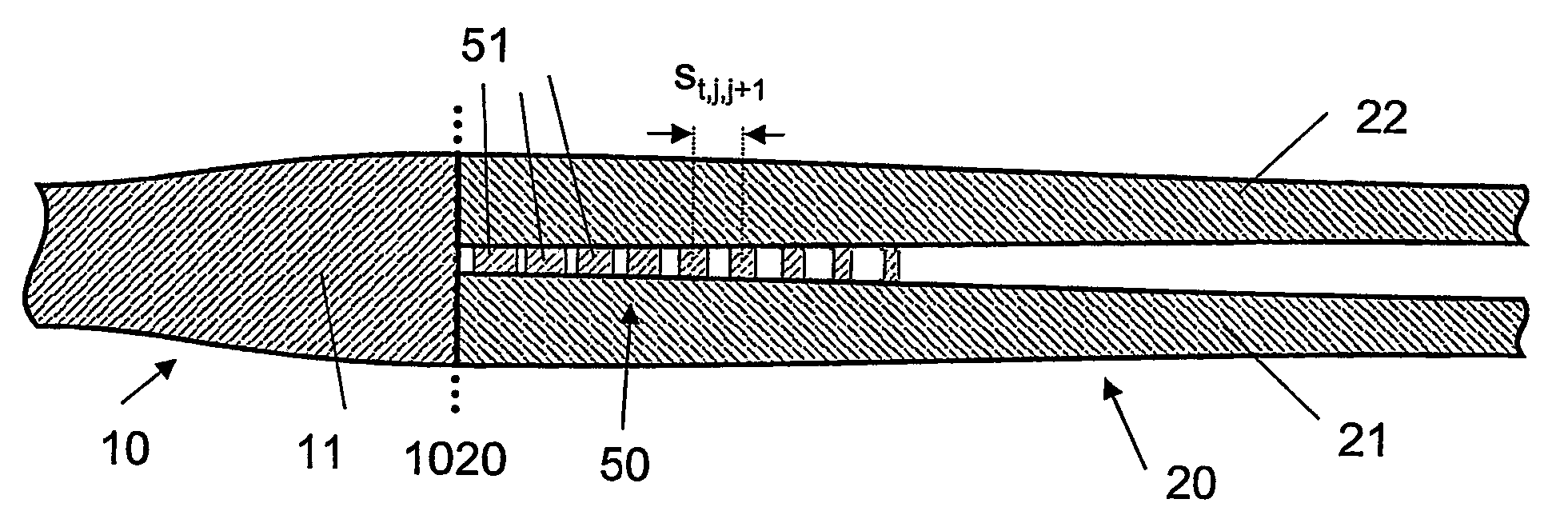
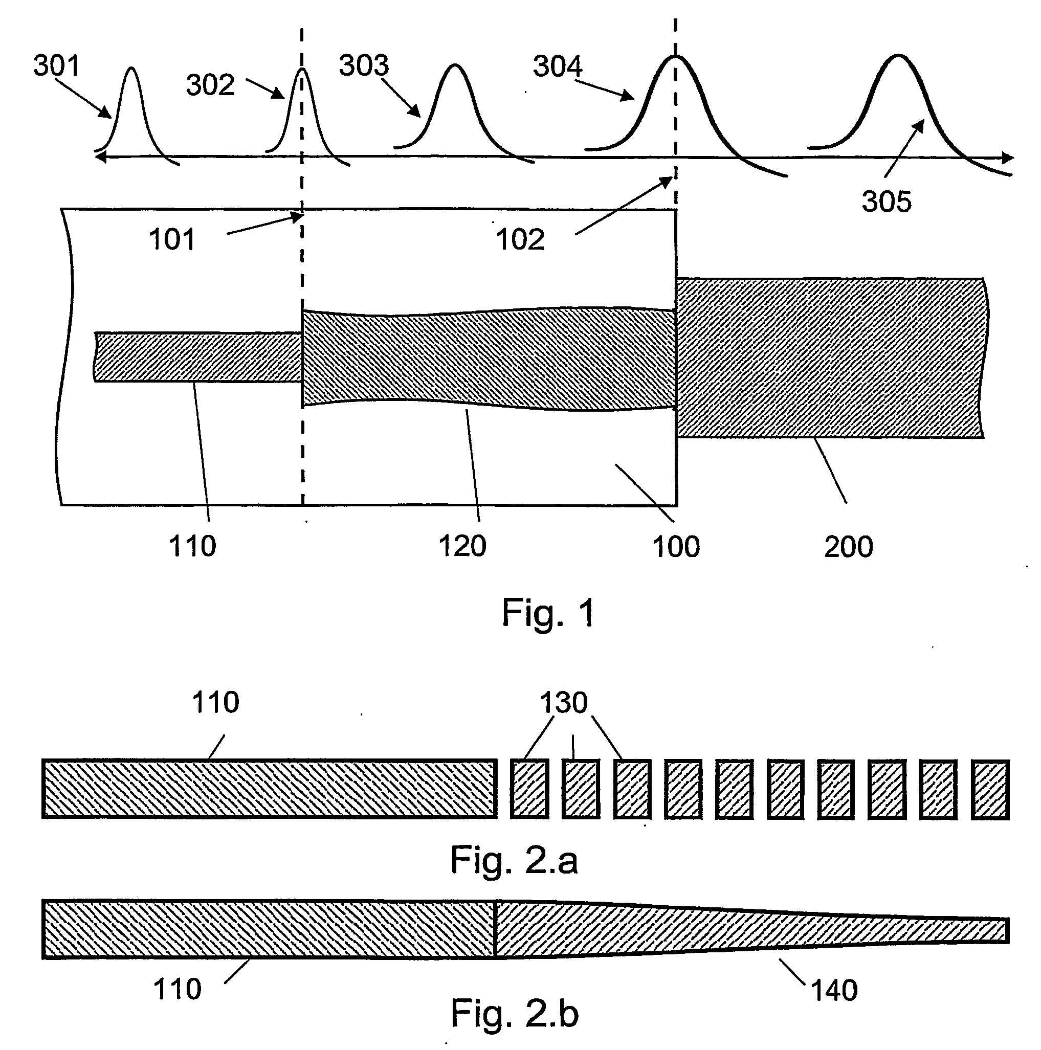
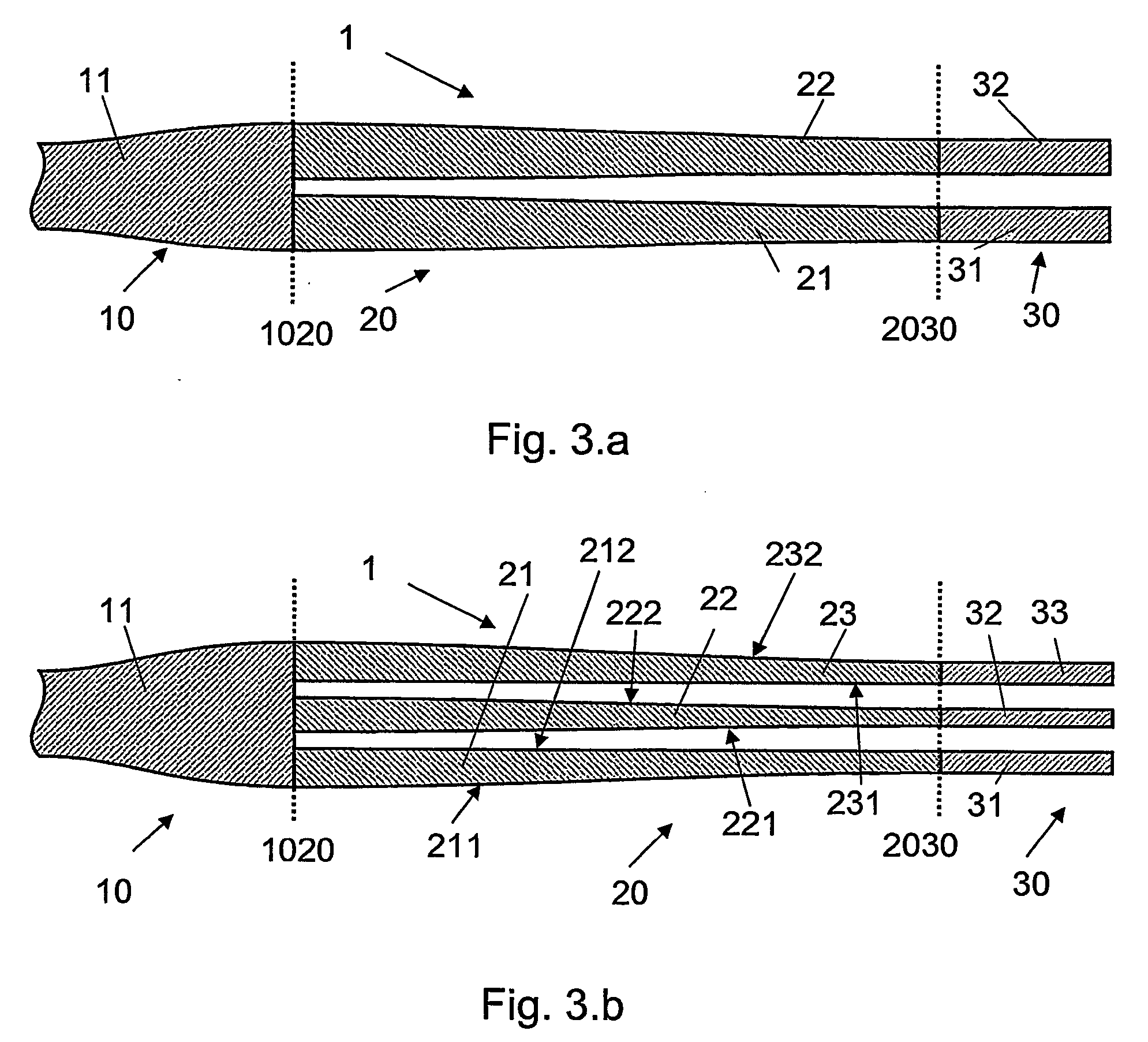
[0179] This example will focus on how to fabricate a specific spot-size converter (as e.g. schematically illustrated in FIG. 3.a or FIG. 8.h). The spot-size converter consists of a taper (termed section 1 above) that transforms the fundamental mode from one width W1 to another width W2, followed by two arms (termed section 2 above) that further propagate and shape the mode such that it as far as possible resembles the mode of an output waveguide typically of different origin (e.g. an optical fibre) as compared to the one of width W1.

[0180] For the sake of simplicity said two arms are made from tapered cosines, but may also be made from adiabatic tapered 5'th or 7'th order polynomials (cf. examples 1 and 2 above).

[0181] The tapered cosine waveguide is described by the area between an upper curve U(z), and a lower curve L(z), where U⁡(z)=x⁡(z)+W⁡(z)2L⁡(z)=x⁡(z)-W⁡(z)2

where x(z) is the centre line, and W(z) is the position dependent width of the waveguide taper x⁡(z)=H2⁢(1-cos⁢ ⁢{...


PUM


Abstract

The invention relates to an optical component (1) comprising a combination of optical waveguide elements for modifying the spot size of a mode of an electromagnetic field propagated by an optical waveguide element, the optical waveguide elements being formed on a substrate. The object of the present invention is to provide a mode coupler with low coupling loss that is easy to manufacture and process tolerant. The problem is solved in that the optical component further comprises a) a first section (10), comprising a first optical waveguide element (11) adapted to sustain at least one mode of the electromagnetic field, b) a second section (20) comprising at least two cooperating optical waveguide elements (21, 22), each of said at least two cooperating optical waveguide elements comprising at least one waveguide segment, said at least two cooperating optical waveguide elements being optically connected to said first optical waveguide element of said first section; wherein said cooperating optical waveguide elements (21, 22) of said second section (20) are adapted to maintain optical coupling between said optical waveguide elements to ensure that said at least one mode of the electromagnetic field is sustained by said at least two cooperating optical waveguide elements in cooperation. Preferably, the waveguides of the first and/or second sections are tapered according to a cosine function or to a 5th or 7th order polynomial. An advantage of an optical component according to the invention is that it provides a mode size converter that is relatively simple to manufacture in that it requires no extra process steps. A further advantage is that it is readily suitable for integration with other optical circuitry on a common substrate. The invention may be used in optical communication systems (e.g. systems employing WDM) where coupling of light between integrated optical circuits and optical fibres are needed.

Description

[0001] This is a nationalization of PCT / DK04 / 000555 filed 19 Aug. 2004 and published in English. This is also claiming the priority of Denmark application PA 2003 01183 filed 19 Aug. 2003 and U.S. Provisional Application No. 60 / 496,010 filed 19 Aug. 2003 under 35 U.S.C. §119.TECHNICAL FIELD [0002] The invention relates to an optical component comprising a combination of optical waveguide elements for modifying the spot size of a mode of an electromagnetic field propagated by an optical waveguide element, the optical waveguide elements being formed on a substrate [0003] The invention further relates to a method of manufacturing an optical component. [0004] The invention may e.g. be useful in applications such as optical communication systems (e.g. systems employing WDM) where coupling of light between integrated optical circuits and optical fibres are needed. BACKGROUND ART [0005] Guided wave optical structures / circuits are typically optical fibres and planar integrated optical waveg...

Claims


Application Information

Patent Timeline
IPC IPC(8): G02B6/26G02B6/12G02B6/122G02B6/30
CPCG02B6/1228G02B6/136G02B6/305G02B2006/1215
Inventor LAURENT-LUND, CHRISTIANAAEN ANDERSEN, LARS-ULRIK
Owner IGNIS PHOTONYX AS
Why Eureka
Try Eureka