Film formation method and apparatus for semiconductor process

a film and semiconductor technology, applied in the direction of wing accessories, door/window fittings, coatings, etc., can solve the problems of increasing parasitic capacitance, increasing background level, and deteriorating inter-substrat uniformity in the composition of deposited films, so as to improve the uniformity of inter-substrat composition

Inactive Publication Date: 2006-09-21
TOKYO ELECTRON LTD
View PDF7 Cites 252 Cited by
  • Summary
  • Abstract
  • Description
  • Claims
  • Application Information

AI Technical Summary

Benefits of technology

[0011] An object of the present invention is to provide an apparatus and method for a semiconductor process, which can uniformly supply a process gas in a small amount, such as a doping gas, into a process container in the vertical direction, thereby improving the inter-substrate uniformity in the composition of deposited films.

Problems solved by technology

In this respect, silicon nitride films have a relatively high dielectric constant, which increases parasitic capacitance and thus is problematic.
Further, where a silicon nitride film is used for a sensor of the charge storage type, there is a problem in that parasitic capacitance increases a background level.
However, as described later, the present inventors have found that, where a process gas in a small amount, such as a doping gas, is used in conventional vertical heat-processing apparatuses (of the so-called batch type), the inter-substrate uniformity in the composition of deposited films tends to be deteriorated.

Method used


Image

  • Film formation method and apparatus for semiconductor process
  • Film formation method and apparatus for semiconductor process
  • Film formation method and apparatus for semiconductor process

Examples


first embodiment

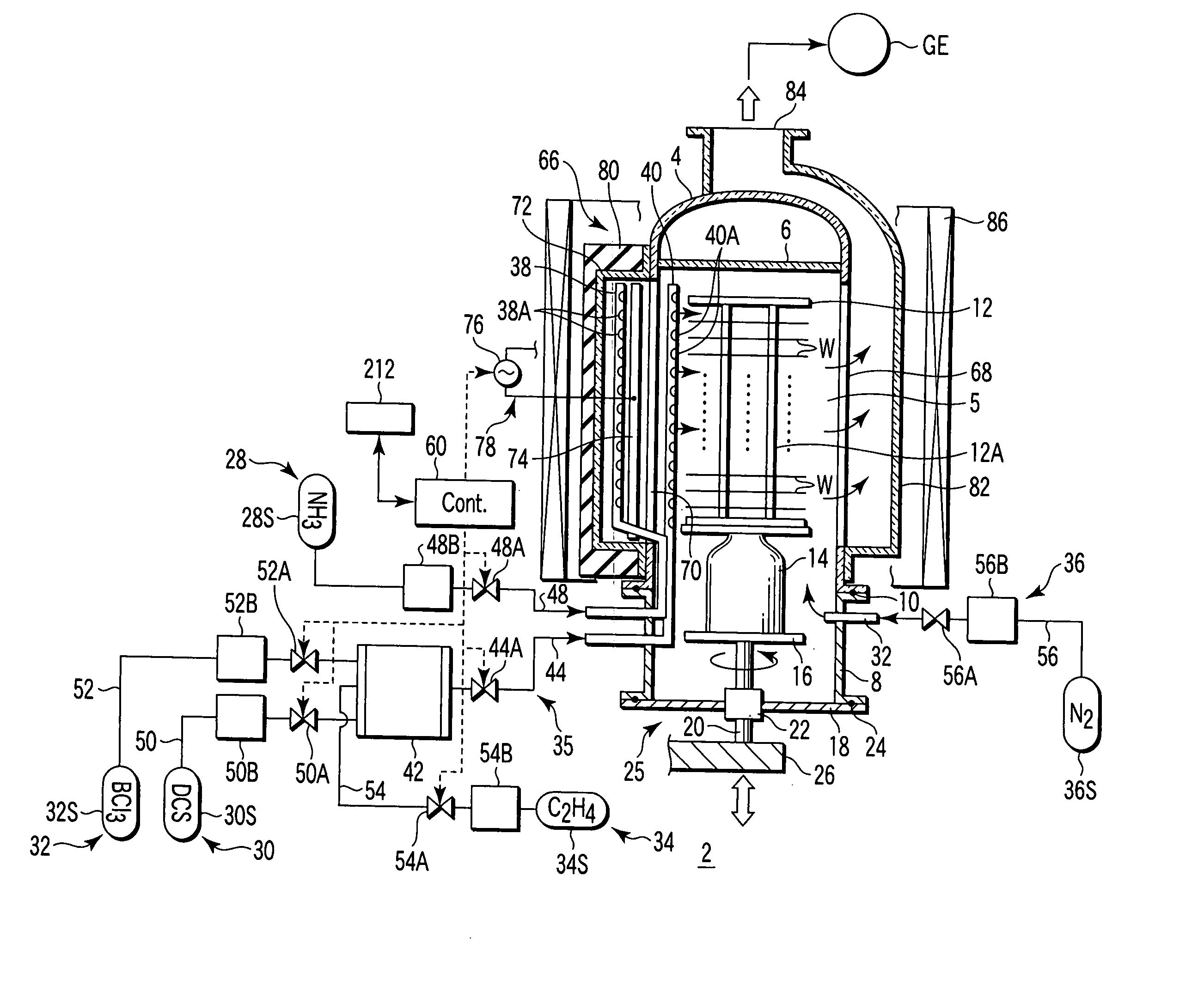
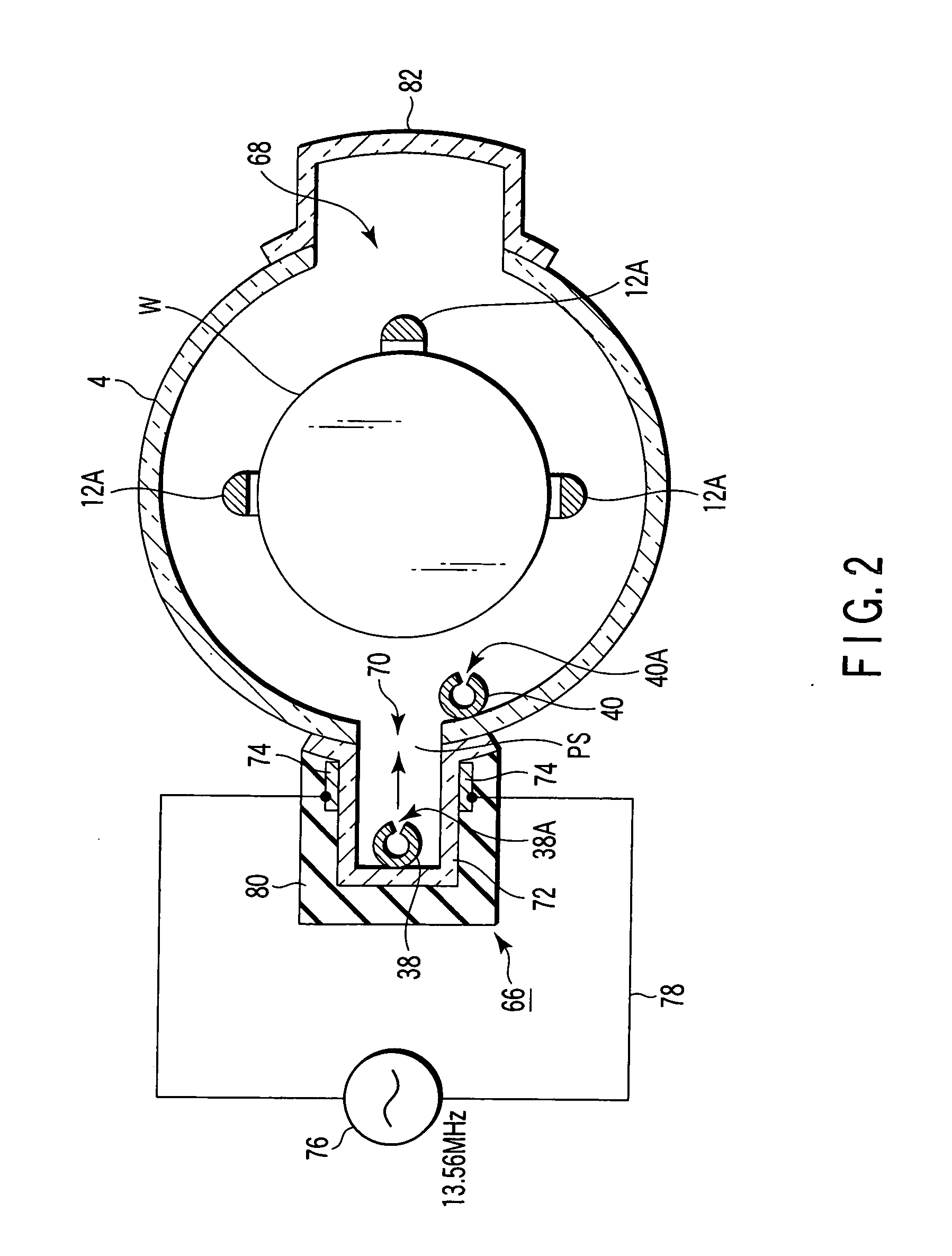
[0084]FIG. 1 is a sectional view showing a film formation apparatus (vertical CVD apparatus) according to the present invention. FIG. 2 is a sectional plan view showing part of the apparatus shown in FIG. 1. The film formation apparatus 2 has a process field configured to be selectively supplied with a first process gas containing dichlorosilane (DCS) gas as a silane family gas, a second process gas containing ammonia (NH3) gas as a nitriding gas, and a third process gas containing BCl3 gas as a boron-containing gas. The film formation apparatus 2 is configured to form an SIBN (boron doped silicon nitride) film on target substrates by CVD in the process field. Accordingly, the boron-containing gas is used as a doping gas. The process field is further configured to be selectively supplied with a fourth process gas containing C2H4 gas (ethylene gas) as a carbon hydride gas, as needed.

[0085] The apparatus 2 includes a process container 4 shaped as a cylindrical column with a ceiling an...

second embodiment

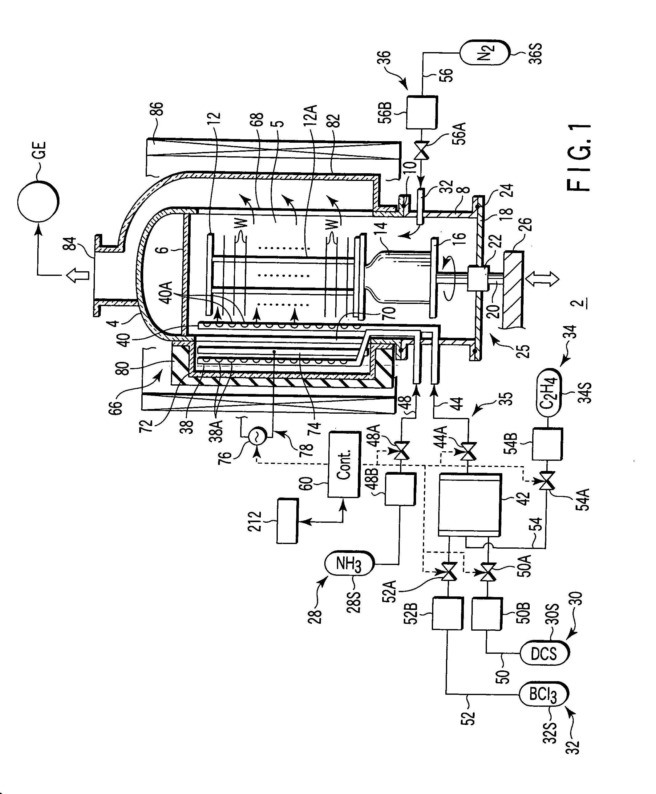
[0125]FIG. 4 is a sectional view showing a film formation apparatus (vertical CVD apparatus) according to the present invention. This film formation apparatus 2X has the same structure as the film formation apparatus 2 shown in FIG. 1 except for the first, third, and fourth process gas supply circuits 30, 32, and 34 and the mixture gas supply circuit 35. Accordingly, an explanation will be give of the film formation apparatus 2X, focusing on the difference from the film formation apparatus 2.

[0126] In the film formation apparatus 2X, the first, third, and fourth process gas supply circuits 30, 32, and 34 are connected to a common mixture gas supply circuit 35X. The mixture gas supply circuit 35X includes a mixture gas supply pipe 40X configured to mix the first and third process gases, and further the fourth process gas in addition thereto, as needed. The mixture gas supply pipe 40X is formed of a quartz pipe, which is a proximal end portion of a gas distribution nozzle 40.

[0127] T...


PUM

PropertyMeasurementUnit
diameteraaaaaaaaaa
volumeaaaaaaaaaa
frequencyaaaaaaaaaa

Abstract

A film formation apparatus for a semiconductor process includes a process gas supply system configured to supply process gases. The process gas supply system includes a gas mixture tank configured to mix first and third process gases to form a mixture gas, a mixture gas supply line configured to supply the mixture gas from the gas mixture tank to a process field, a second process gas supply circuit having a second process gas supply line configured to supply a second process gas to the process field without passing through the gas mixture tank, and first and second switching valves disposed on the mixture gas supply line and the second process gas supply line, respectively. A control section controls the first and second switching valves to be opened and closed so as to alternately and pulse-wise supply the mixture gas and the second process gas to the process field.

Description

CROSS-REFERENCE TO RELATED APPLICATIONS [0001] This application is based upon and claims the benefit of priority from prior Japanese Patent Applications No. 2005-070034, filed Mar. 11, 2005; and No. 2006-004192, filed Jan. 11, 2006, the entire contents of both of which are incorporated herein by reference. BACKGROUND OF THE INVENTION [0002] 1. Field of the Invention [0003] The present invention relates to a film formation apparatus and method for a semiconductor process for forming a thin film on a target substrate, such as a semiconductor wafer. The term “semiconductor process” used herein includes various kinds of processes which are performed to manufacture a semiconductor device or a structure having wiring layers, electrodes, and the like to be connected to a semiconductor device, on a target substrate, such as a semiconductor wafer or a glass substrate used for an LCD (Liquid Crystal Display) or FPD (Flat Panel Display), by forming semiconductor layers, insulating layers, and ...

Claims


Application Information

Patent Timeline
Patent Type & Authority Applications(United States)
IPC IPC(8): C23C16/00
CPCC23C16/345C23C16/45512C23C16/45531C23C16/45542C23C16/45578C23C16/509C23C16/45553H01L21/0217H01L21/02274H01L21/0228H01L21/02211H01L21/02219
Inventor HASEBE, KAZUHIDEOKADA, MITSUHIROKIM, CHAEHOLEE, BYOUNGHOONCHOU, PAO-HWA
Owner TOKYO ELECTRON LTD
Why Eureka
Try Eureka