

SOS wafer and manufacturing method thereof
- Summary
- Abstract
- Description
- Claims
- Application Information
AI Technical Summary
Benefits of technology
Problems solved by technology
Method used
Image

Examples
first preferred embodiment
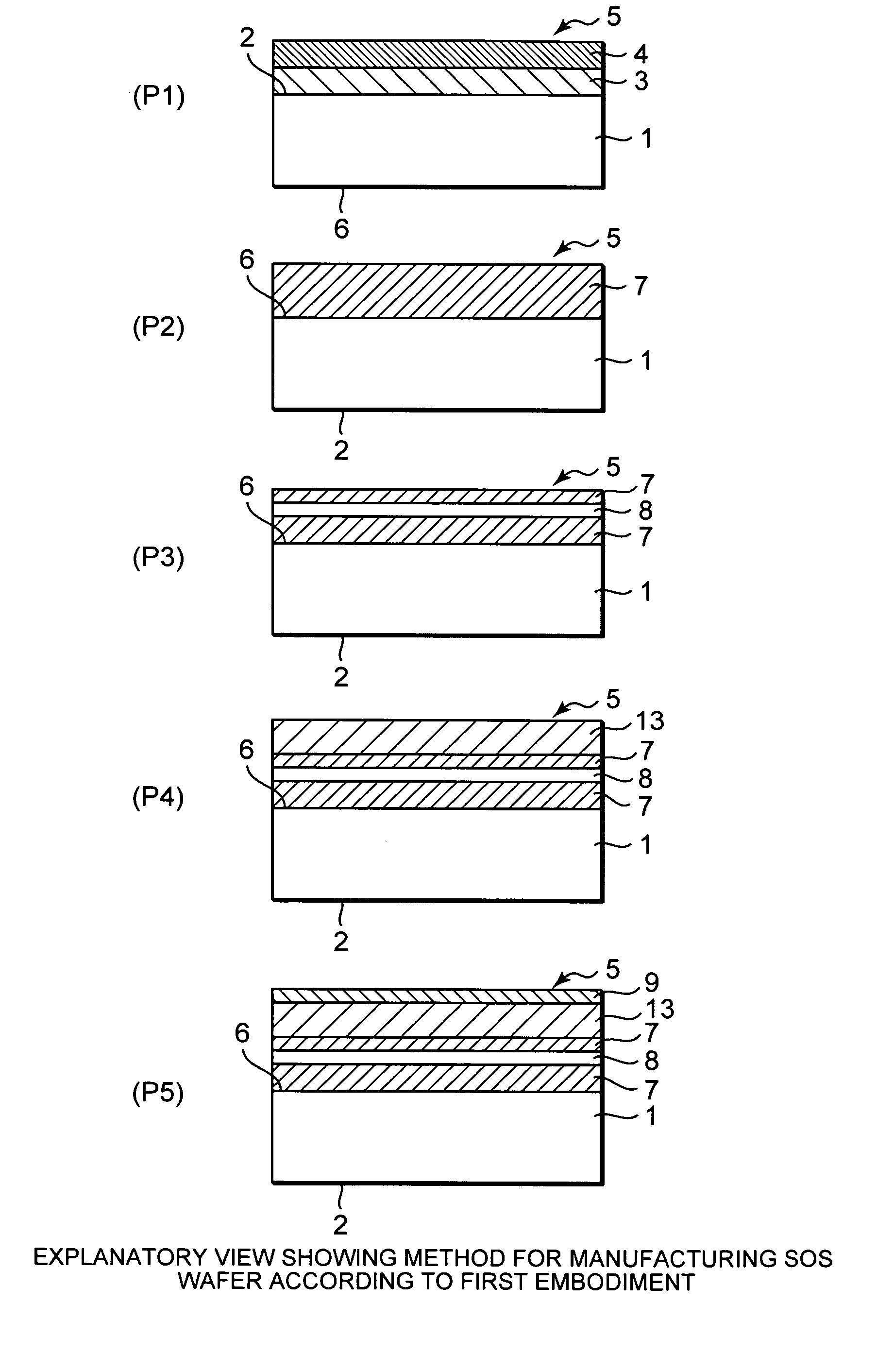
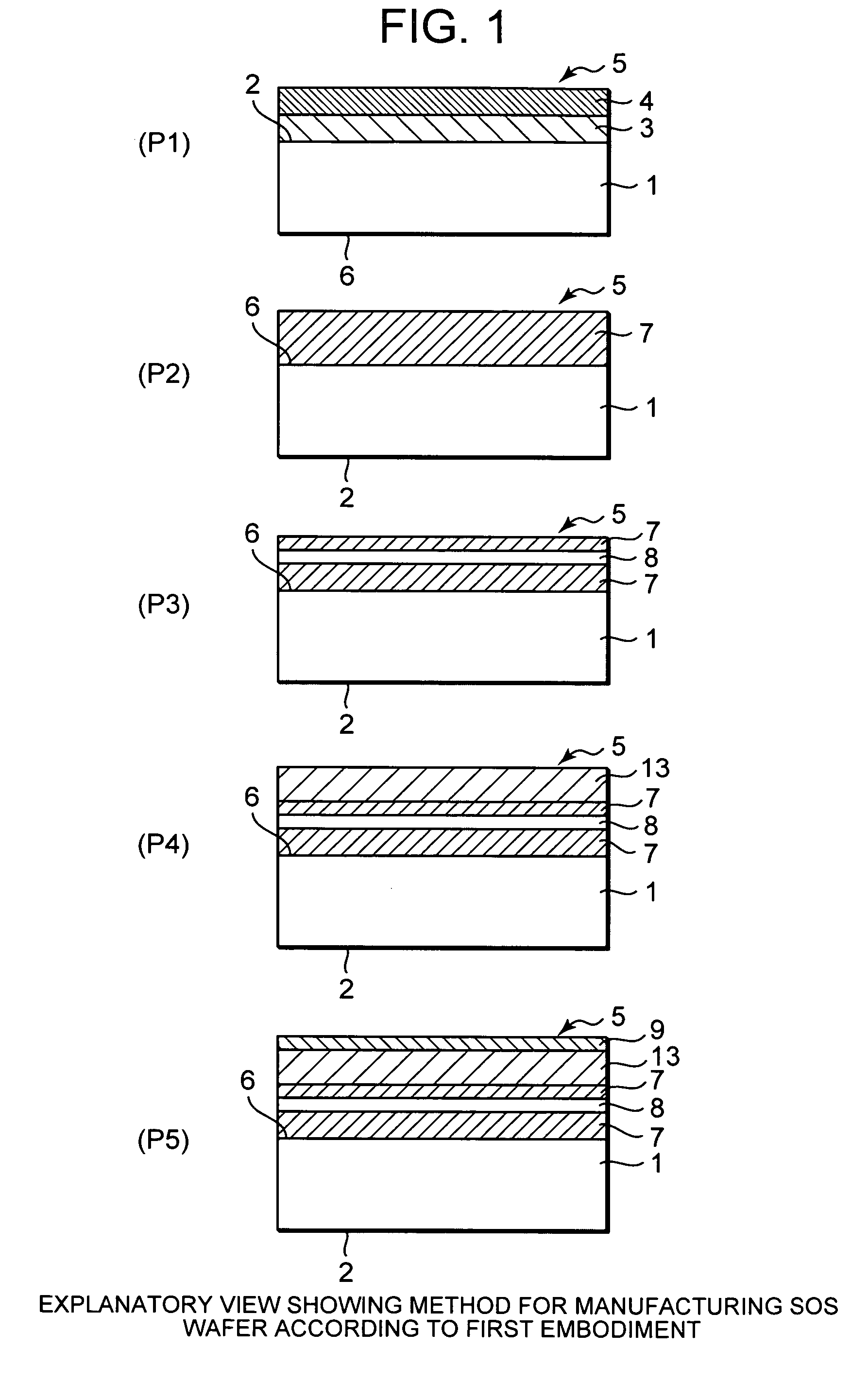
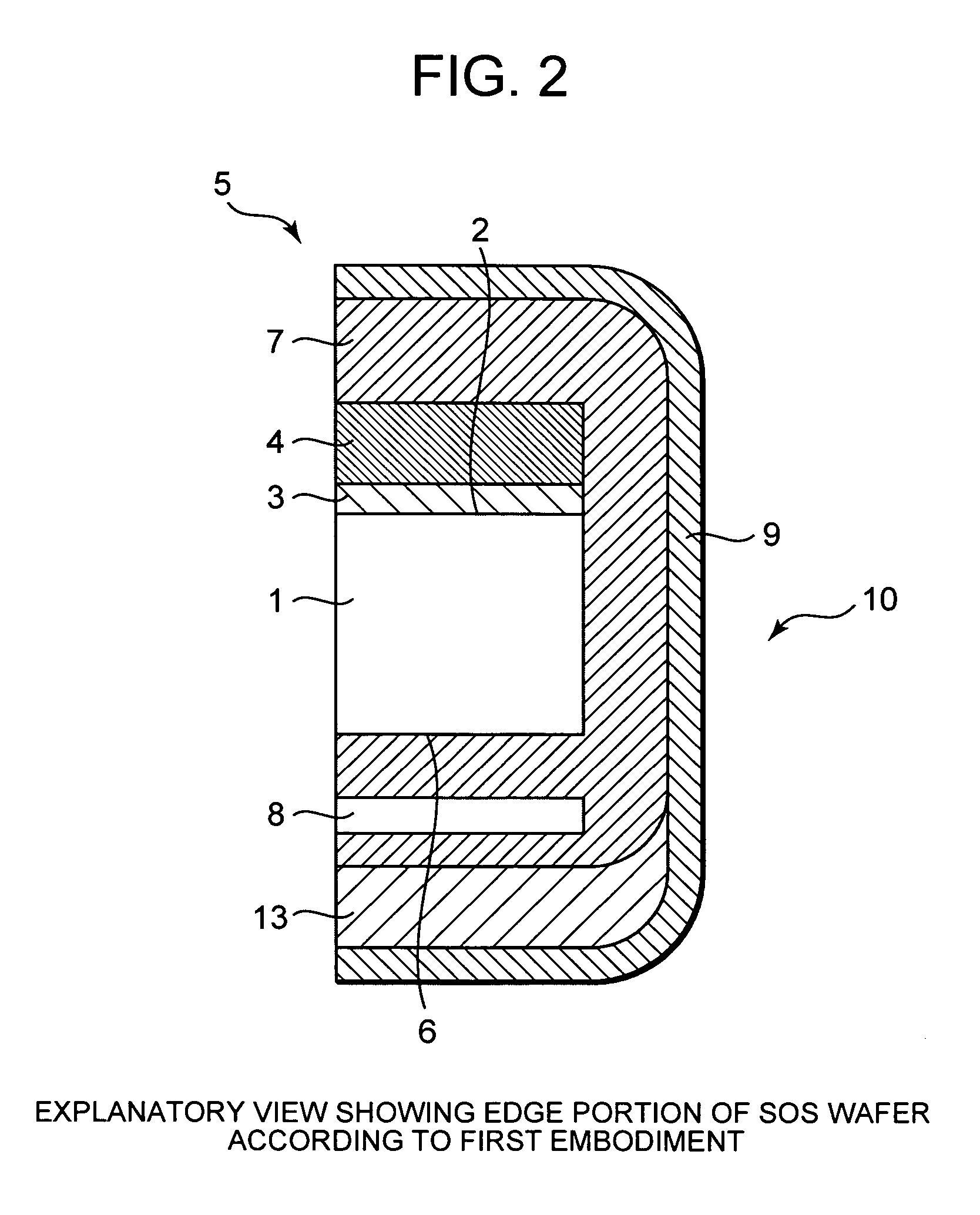
[0045]FIG. 1 is an explanatory view showing a method for manufacturing an SOS wafer according to a first embodiment, and FIG. 2 is an explanatory view illustrating an edge portion of the SOS wafer according to the first embodiment, respectively.
[0046] Incidentally, constituent elements similar to those employed in the prior art are given the same reference numerals, and their explanations will therefore be omitted.
[0047] In FIG. 1, reference numeral 13 indicates a silicon nitride film used as a stress relaxing film, which is deposited or grown by a plasma CVD method using a parallel plate type plasma CVD (Chemical Vapor Deposition) apparatus.
[0048] A silicon layer 3 formed in a front surface 2 of a sapphire substrate 1 employed in the present embodiment is a silicon layer monocrystallized by epitaxial growth. The method for manufacturing the SOS wafer according to the present embodiment will be explained below in accordance with processes or process steps indicated by P using FIG...
second preferred embodiment
[0069]FIG. 3 is an explanatory view showing a method for manufacturing an SOS wafer according to a second embodiment, and FIG. 4 is an explanatory view showing an edge portion of the SOS wafer according to the second embodiment, respectively.
[0070] Incidentally, constituent elements similar to those employed in the first embodiment are given the same reference numerals, and their explanations will therefore be omitted.
[0071] The method for manufacturing the SOS wafer according to the present embodiment will hereinafter be described in accordance with processes or process steps indicated by PA using FIG. 3.
[0072] In PA1, an SOS wafer 5 in which a silicon layer 3 and an oxide layer 4 are laminated over a front surface 2 of a sapphire substrate 1, is prepared in a manner similar to the process step P1 of the first embodiment.
[0073] In PA2, a polysilicon layer 7 is formed over a back surface 6 of the sapphire substrate 1 and the oxide layer 4 on the front surface 2 side and at each ...
third preferred embodiment
[0085]FIG. 5 is an explanatory view showing a method for manufacturing an SOS wafer according to a third embodiment, and FIG. 6 is an explanatory view showing an edge portion of the SOS wafer according to the third embodiment, respectively.
[0086] Incidentally, constituent elements similar to those employed in the first embodiment are given the same reference numerals, and their explanations will therefore be omitted.
[0087] In FIG. 5, reference numeral 15 indicates a silicon oxide film used as a stress relaxing film, which is deposited by a plasma CVD method using a parallel plate type plasma CVD apparatus.
[0088] The method for manufacturing the SOS wafer of the present embodiment will be explained below in accordance with processes or process steps indicated by PB using FIG. 5.
[0089] Since the process steps PB1 through PB3 of the present embodiment are similar to the process steps P1 through P3 of the first embodiment, their explanations are omitted.
[0090] In PB4, a 10000 Å-thi...
PUM
 Abstract
Description
Claims
Application Information