Cascaded light emitting devices based on mixed conductor electroluminescence

a light emitting device and mixed conductor technology, applied in the direction of discharge tube luminescnet screen, discharge tube/lamp details, organic semiconductor devices, etc., can solve the problems of reducing the brightness of an entire panel, affecting the efficiency of light transmission,

Active Publication Date: 2006-09-28
PANASONIC CORP +1
View PDF7 Cites 8 Cited by
  • Summary
  • Abstract
  • Description
  • Claims
  • Application Information

AI Technical Summary

Benefits of technology

[0008] Another exemplary embodiment of the present invention is a cascaded light emitting device. The cascaded light emitting device includes: a split electrode structure formed of a first electrode material; an opposing electrode formed of a second electrode material; and at least one electroluminescent layer coupled between the split electrode structure and the opposing electrode. The split electrode structure includes a number of electrode portions. The electrical resistance between any pair of these electrode portions of the split electrode structure is greater than a split resistance. The electrode portions include a first electrode portion that is electrically coupled to a first voltage lead and a second electrode portion that is electrically coupled to a second voltage lead. The electroluminescent layer(s) includes a mixed conductor that luminesces with a peak wavelength. A total thickness of the electroluminescent layer(s) is such that a resistance across the electroluminescent layer(s) between an electrode portion of the split electrode structure and the opposing electrode is less than half of the split resistance.
[0009] A further exemplary embodiment of the present invention is a method for driving of an electroluminescent device with an alternating current where the electroluminescent device includes: a first electrode; a second electrode; and at least one electroluminescent layer coupled between the first electrode and the second electrode, which includes a mixed conductor. The electroluminescent device is biased to generate a polarizing voltage across the electroluminescent layer(s) from the first electrode to the second electrode. The polarization voltage is greater than or equal to the voltage necessary to enhance charge injection into the mixed conductor. The potential difference across the electroluminescent layer(s) from the first electrode to the second electrode is maintained above an operational voltage for a predetermined luminescence period. The operational voltage is less than or equal to the polarizing voltage and greater than or equal to the voltage necessary to drive electroluminescence in the polarized mixed conductor. The electroluminescent device is biased to generate the polarizing voltage across the electroluminescent layer(s) from the second electrode to the first electrode and the potential difference across the electroluminescent layer(s) from the second electrode to the first electrode is maintained above an operational voltage for the predetermined luminescence period. The steps are then repeated.

Problems solved by technology

However, a number of issues remain before OLED-based displays are able to reach their full potential.
In a passive matrix architecture, a short may cause all pixels that share the same row and column electrodes to stay dark, thus potentially dramatically decreasing the brightness of an entire panel.
For a flat panel display, the loss of a large number of pixels due to a short in one OLED may lead to unacceptable image degradation.
The active matrix architecture does not suffer from this shortfall; however, it can be expensive and difficult to implement this architecture over arbitrarily large areas.
However, this architecture requires patterning of the organic layer, which increases the complexity of the manufacturing process and may lead to additional faults.
This step adds significantly to the complexity and might be detrimental to the speed of display manufacture.
However, this architecture was specifically designed for increasing the efficiency of OLED's and was not meant to provide a fault tolerant way of building large area panels.

Method used


Image

  • Cascaded light emitting devices based on mixed conductor electroluminescence
  • Cascaded light emitting devices based on mixed conductor electroluminescence
  • Cascaded light emitting devices based on mixed conductor electroluminescence

Examples


Embodiment Construction

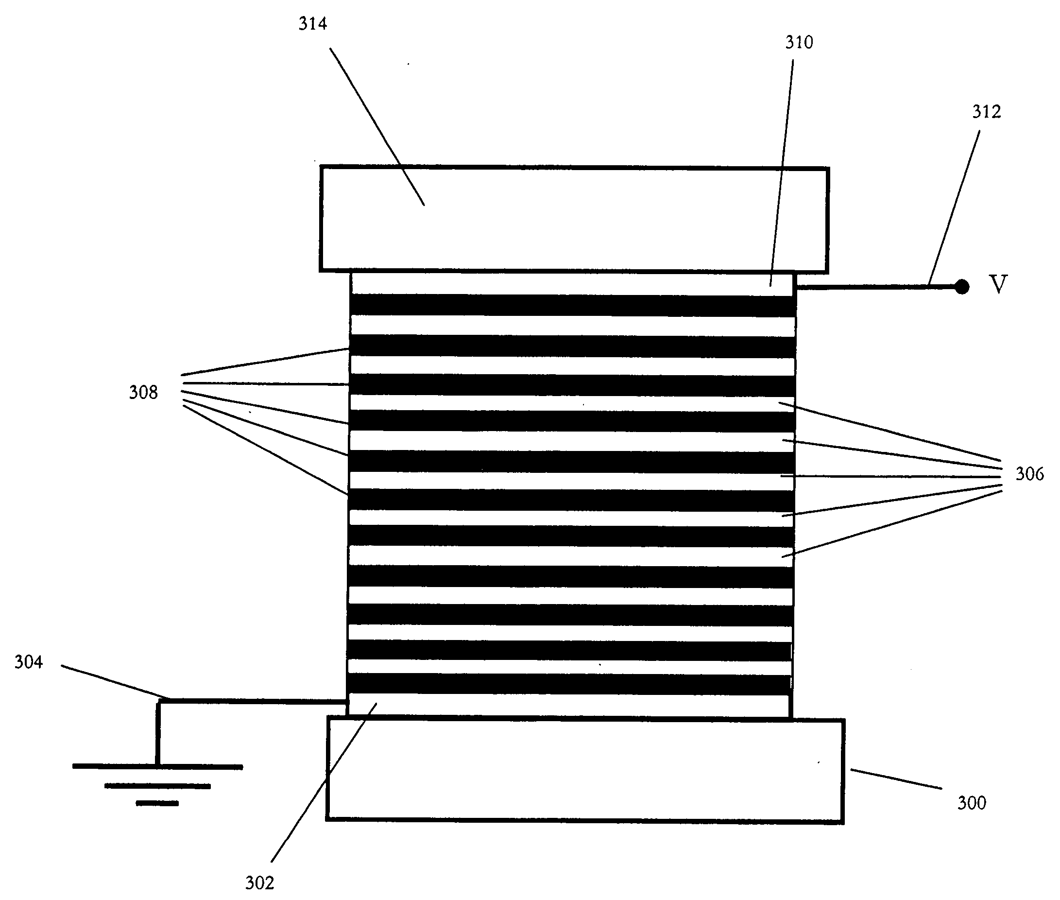
[0022] As discussed above, device architectures involving the series connection of electroluminescent cells in the prior art require patterning not only of the electrodes, but also of the luminescent layer. Additionally in these prior art designs, the resulting light is generated in light emitting diode configurations. Exemplary embodiments of the present invention include stacked and cascaded electroluminescent (OEL) device architectures that do not require patterning of electroluminescent layer. These exemplary device architectures also utilize mixed conductors to produce electroluminescence without the need to produce diode structures. This feature allows the use of alternating current (AC) driving signals in exemplary embodiments of the present invention. Further, the present invention allows a simplified manufacturing process that may provide high yield and reduced manufacturing costs.

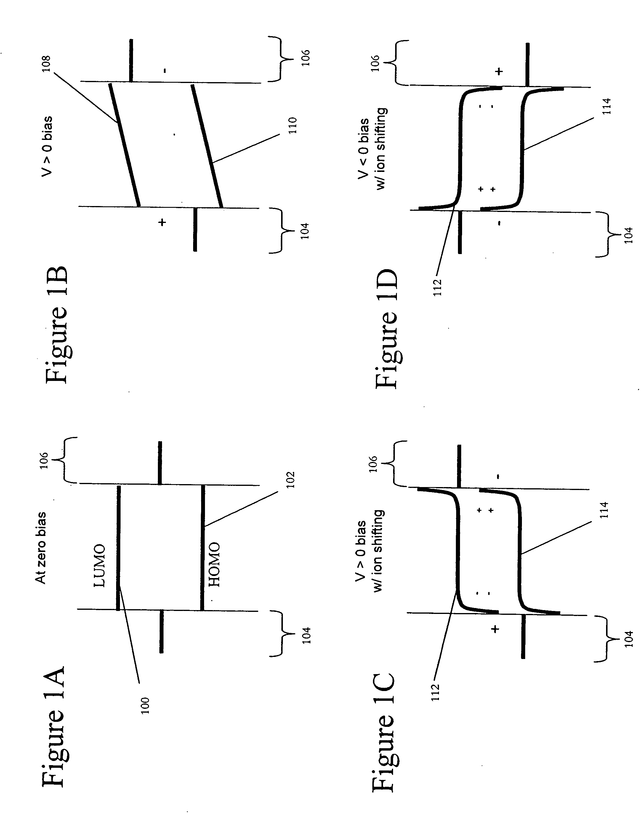
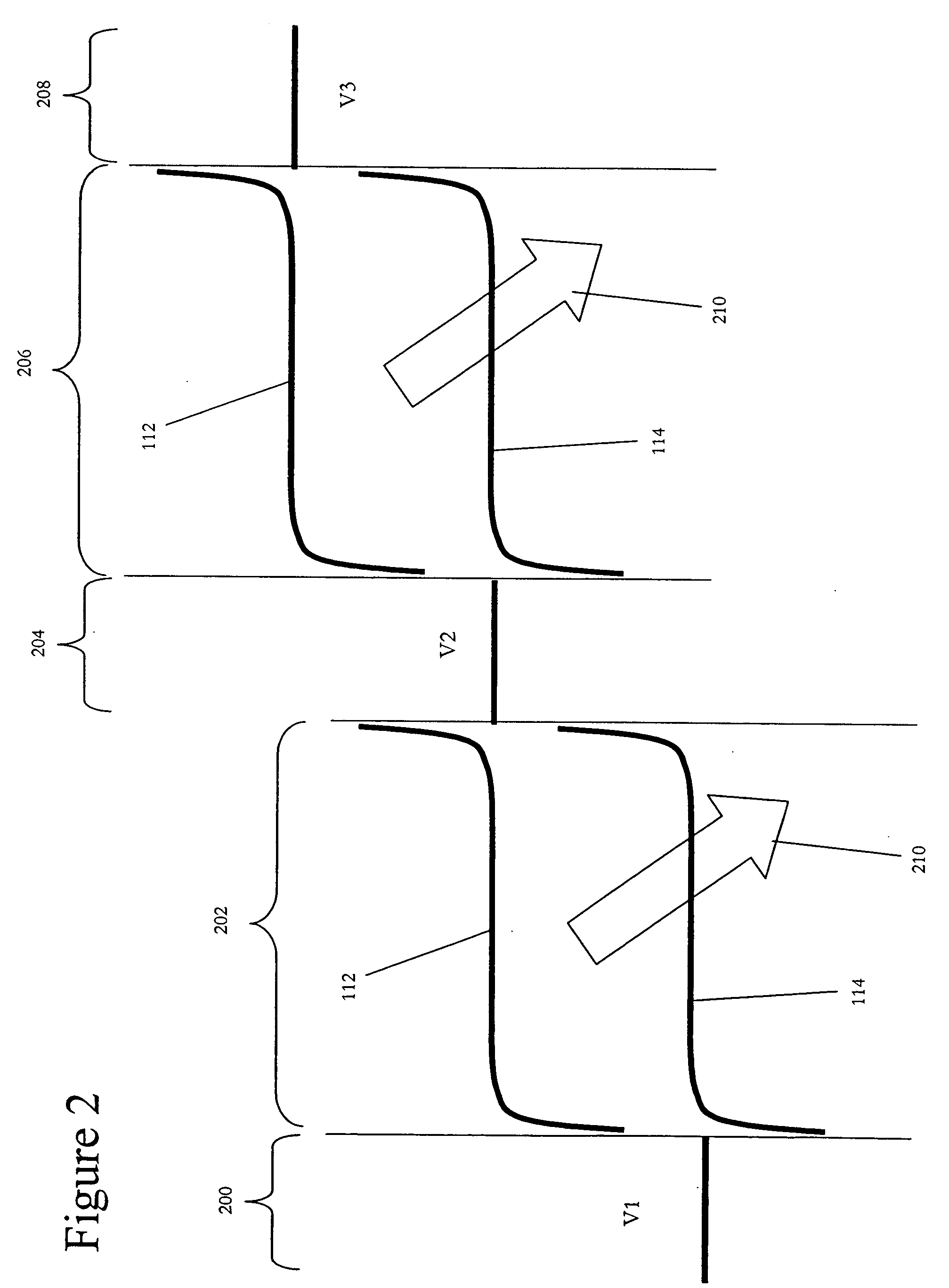
[0023] FIGS. 1A-D are intuitive energy diagrams illustrating some of the desirable properties...


PUM


Abstract

A cascaded light emitting device. The cascaded light emitting device includes: a base electrode formed of a base electrode material and electrically coupled to a base voltage lead; a top electrode layer formed of a top electrode material and electrically coupled to a top voltage lead; a number of electroluminescent layers arranged between and electrically coupled to the base electrode and top electrode layer; and at least one middle electrode layer formed of a middle electrode material. Each of the middle electrodes is coupled between two juxtaposed electroluminescent layers. The electroluminescent layers include a mixed conductor that luminesces with a peak wavelength.

Description

[0001] This work was supported by the National Science Foundation (Career Award DMR-0094047, and ECS-0210693) and by the Cornell Center for Materials Research (CCMR), a Materials Research Science and Engineering Center of the National Science Foundation (DMR-9632275).FIELD OF THE INVENTION [0002] The present invention concerns improved designs for light emitting devices based on electroluminescence. In particular, these designs may allow for the manufacture of displays with increased optical output, improved tolerance to shorts, and the ability to be driven using alternating current. BACKGROUND OF THE INVENTION [0003] Recently, there has been significant interest in organic light emitting diodes (OLED's). These structures have begun entering the flat panel display market. A variety of consumer electronics products, such as car stereos and cell phones, are also available with OLED-based displays. In addition to these uses, a number of other applications, such as large-area signs and ...

Claims


Application Information

Patent Timeline
Patent Type & Authority Applications(United States)
IPC IPC(8): H05B33/14
CPCH01L27/3209H01L51/5032H01L51/5203H01L51/5271H01L51/5278H01L2251/564H10K59/32H10K50/135H10K50/805H10K50/19H10K50/856H10K71/841
Inventor MALLIARAS, GEORGE M.MORI, KIYOTAKASLINKER, JASON D.BERNARDS, DANIEL A.ABRUNA, HECTOR D.
Owner PANASONIC CORP
Why Eureka
Try Eureka