

Light emitting element and method for manufacturing the same
a technology manufacturing methods, which is applied in the direction of discharge tubes/lamp details, discharge tubes luminescent screens, electric discharge lamps, etc., can solve the problems of reducing the luminance of light emitting elements, reducing the adhesion property of electrical components made of ag or al, and reducing the luminance of electrical components. , to achieve the effect of low contact resistance and high reflectivity
- Summary
- Abstract
- Description
- Claims
- Application Information
AI Technical Summary
Benefits of technology
Problems solved by technology
Method used
Image

Examples
first embodiment
VARIANT OF FIRST EMBODIMENT
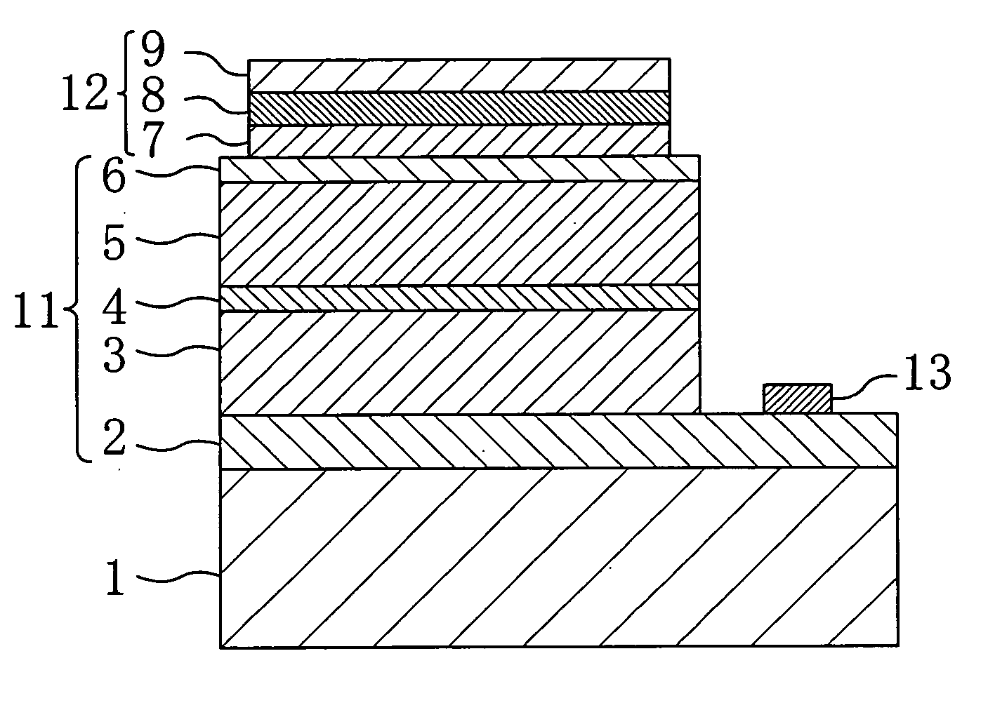
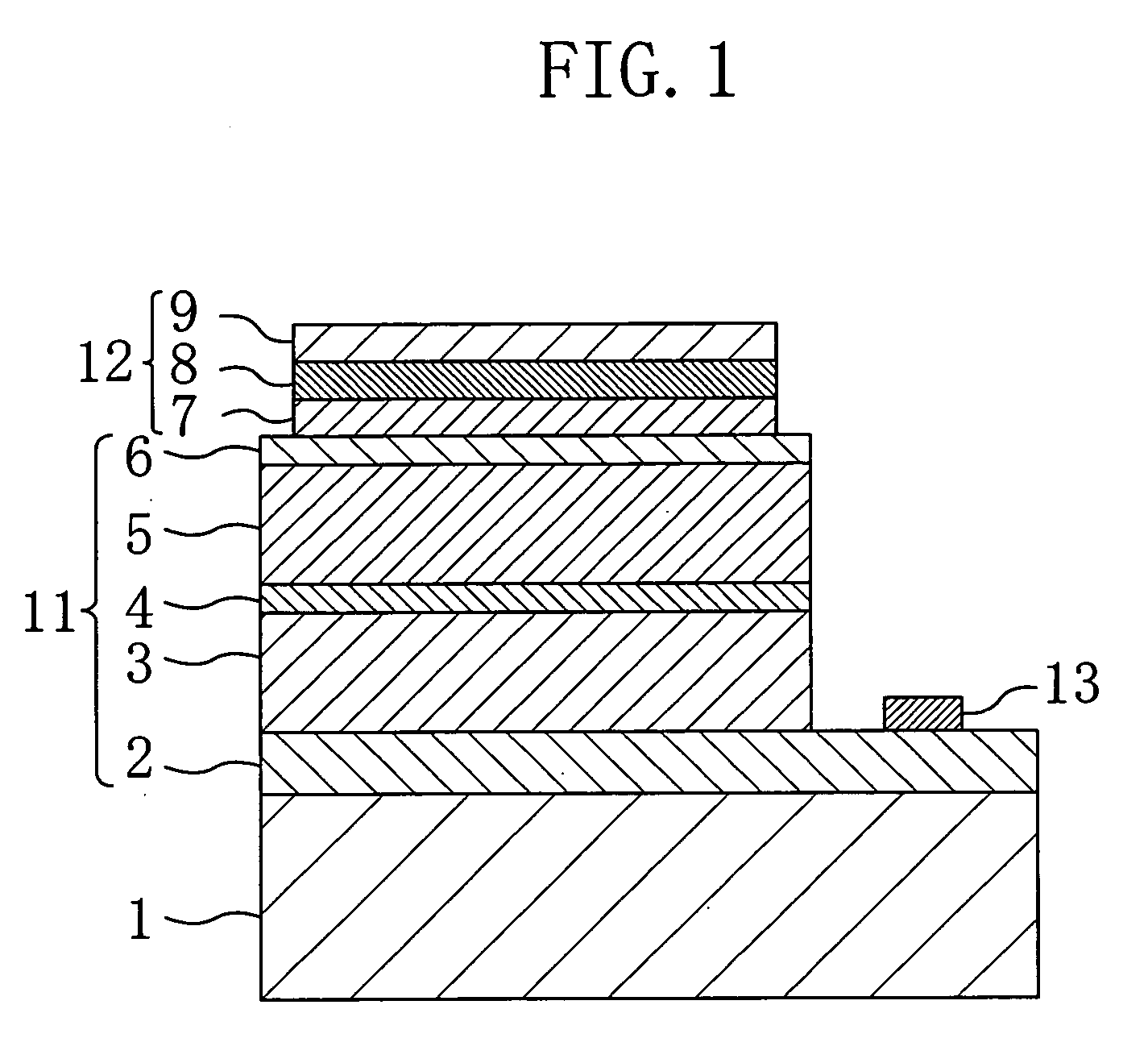
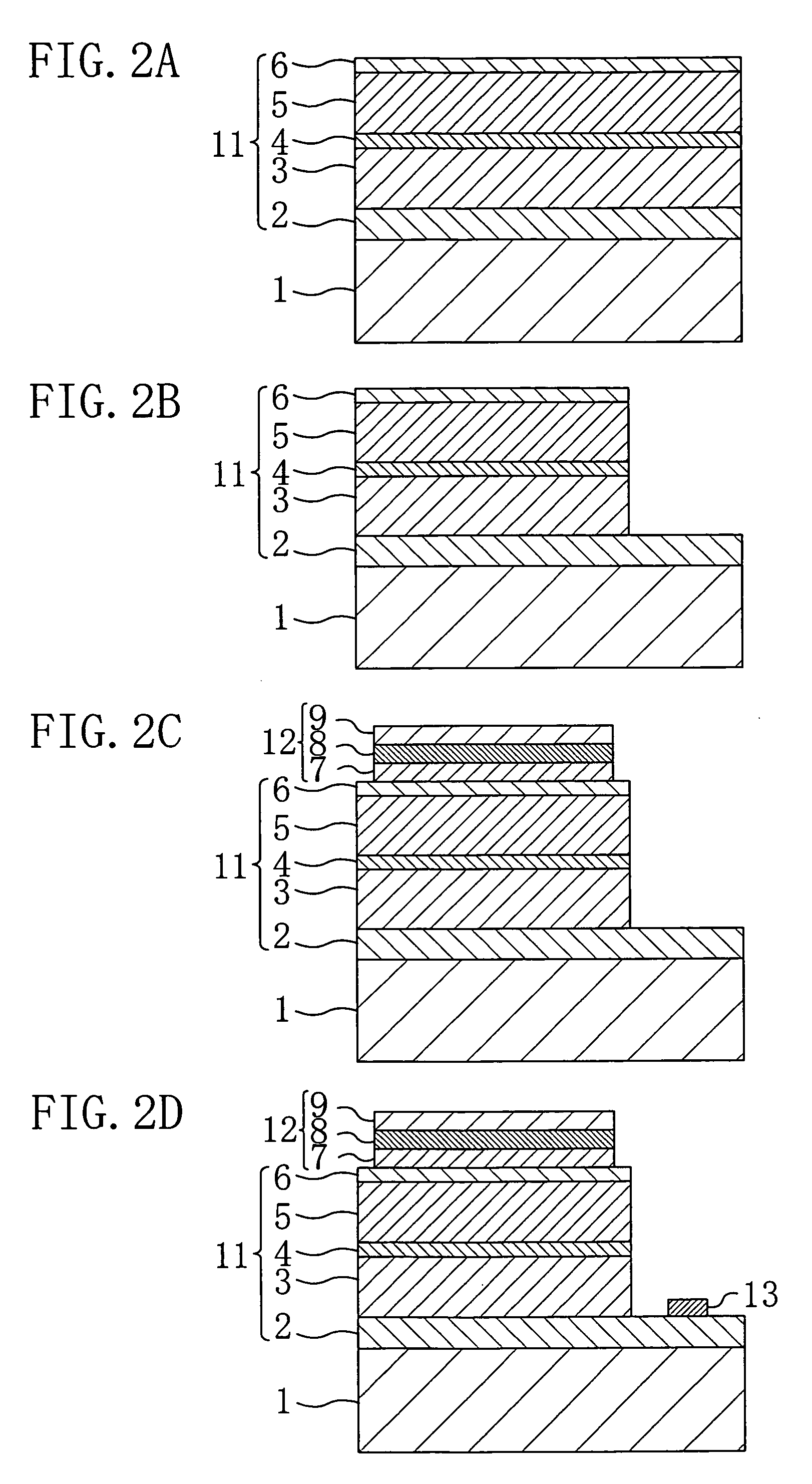
[0064] Hereinafter, an explanation of a light emitting element as a variant of the first embodiment will be provided with reference to the drawings. FIG. 8 is a sectional view illustrating the structure of the variant light emitting element. In FIG. 8, the same components as those shown in FIG. 1 are indicated by the same reference numerals to omit the explanation.
[0065] As shown in FIG. 8, the variant light emitting element includes a 2 nm thick metal contact resistance reducing film 14 which is made of Ni and formed between the p-type contact layer 6 and the metal optical reflection film 7. Therefore, the contact resistance between the p-type contact layer 6 and the p-type electrode 12 is reduced and heat generation in the light emitting element is also reduced.
[0066] The metal contact resistance reducing film 14 may be made of any metal which is capable of forming good contact with a semiconductor layer such as nickel (Ni), platinum (Pt), titanium (Ti...
second embodiment
[0071] An explanation of a light emitting element according to a second embodiment of the present invention and a method for manufacturing the same will be provided with reference to the drawings. FIG. 10 is a sectional view illustrating the structure of the light emitting element according to the second embodiment. As shown in FIG. 10, the light emitting element of the present embodiment is a blue light emitting element using a gallium nitride (GaN)-based material.
[0072] On a conductive substrate 21 made of p-type silicon (Si), a 150 nm thick metal cover film 29 made of Au, a 100 nm thick metal anti-diffusion film 28 made of W and a 150 nm thick metal optical reflection film 27 made of Ag are formed in this order to provide a p-type electrode 32.
[0073] On the p-type electrode 32, a p-type contact layer 26 made of p-type GaN, a p-type cladding layer 25 made of p-type aluminum gallium nitride (Al0.1Gao0.9N), a light emitting layer 24, an n-type cladding layer 23 made of n-type Al0....
PUM
 Abstract
Description
Claims
Application Information