
Semiconductor integrated circuit

a technology of integrated circuits and semiconductors, applied in the field of semiconductor integrated circuits, can solve the problems of reducing snm, multi-bit error in which a plurality of cells generate an error simultaneously, inversion of logical data stored in memory cells, etc., and achieve the effect of improving processing accuracy and soft error toleran

Inactive Publication Date: 2006-09-28
RENESAS ELECTRONICS CORP
View PDF6 Cites 34 Cited by
  • Summary
  • Abstract
  • Description
  • Claims
  • Application Information

AI Technical Summary

Benefits of technology

[0014] The present invention can provide a semiconductor integrated circuit that improves soft error tolerance and enables to improve processing accuracy.

Problems solved by technology

Meanwhile in recent years as elements become finer, soft error phenomena are reported to occur that causes an inversion of logical data stored in a memory cell due to an influence of radiation such as neutrons from cosmic radiation that reach on the ground.
Moreover the influence of radiation further causes a multi-bit error in which a plurality of cells generate an error simultaneously.
Since noise on the bit line can be also easily transmitted, it could result in a decrease of SNM, generating a bias in a stability point, and cell data being easily destroyed.
For this reason, a transfer transistor is usually designed to have an inferior capability than a driver transistor.
For a SRAM memory cell that induces a difference in drive capability by differentiating a gate length of a driver transistor from that of a transfer transistor as described by Satomi et al., there could be a difficulty in reducing cell area due to nonuniformity in its pattern.
It could also reduce accuracy in microfabrication.
However it has now been discovered that no technique has considered over both of a layout in view of processing accuracy and a reduction in charge collection of cell node diffusion layer on a radiation incidence.

Method used


Image

  • Semiconductor integrated circuit
  • Semiconductor integrated circuit
  • Semiconductor integrated circuit

Examples


Embodiment Construction

[0022] The invention will be now described herein with reference to illustrative embodiments. Those skilled in the art will recognize that many alternative embodiments can be accomplished using the teachings of the present invention and that the invention is not limited to the embodiments illustrated for explanatory purposed.

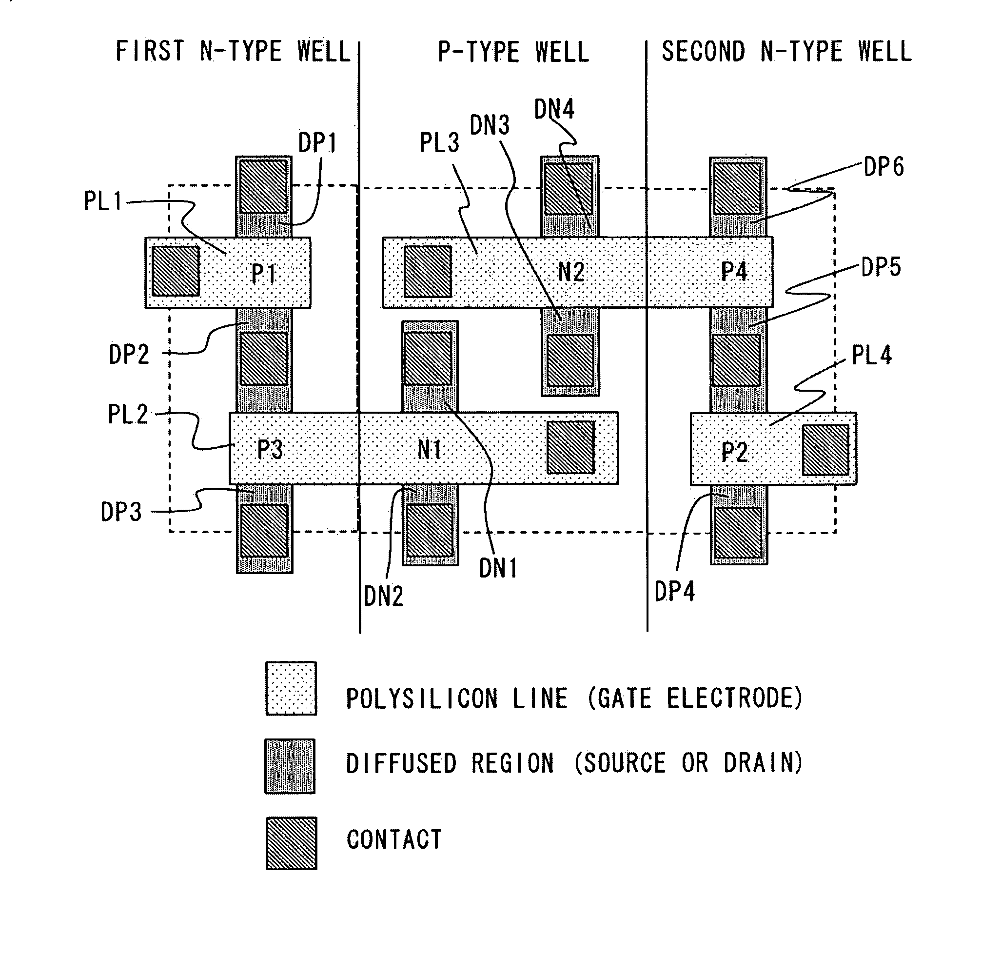
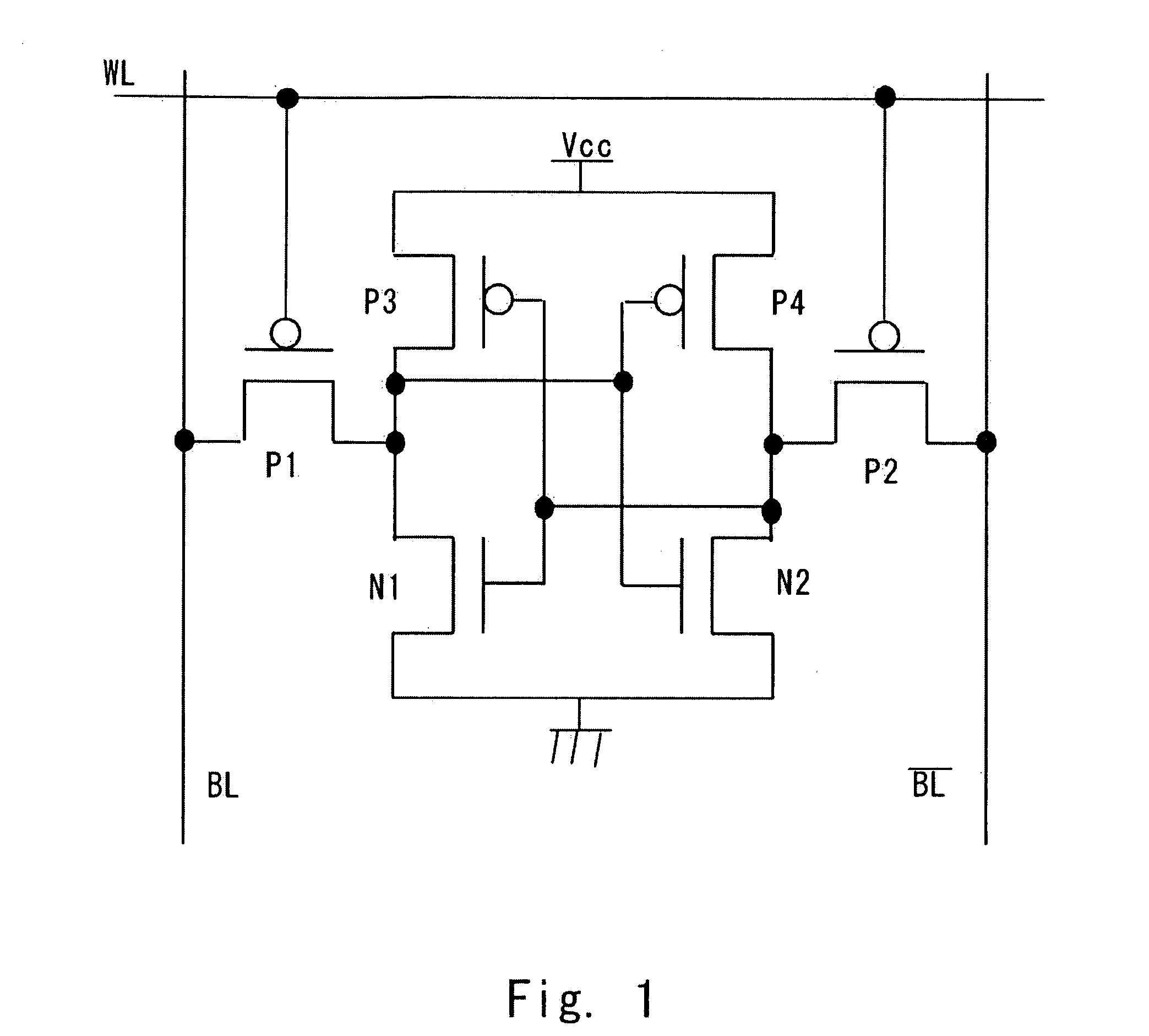
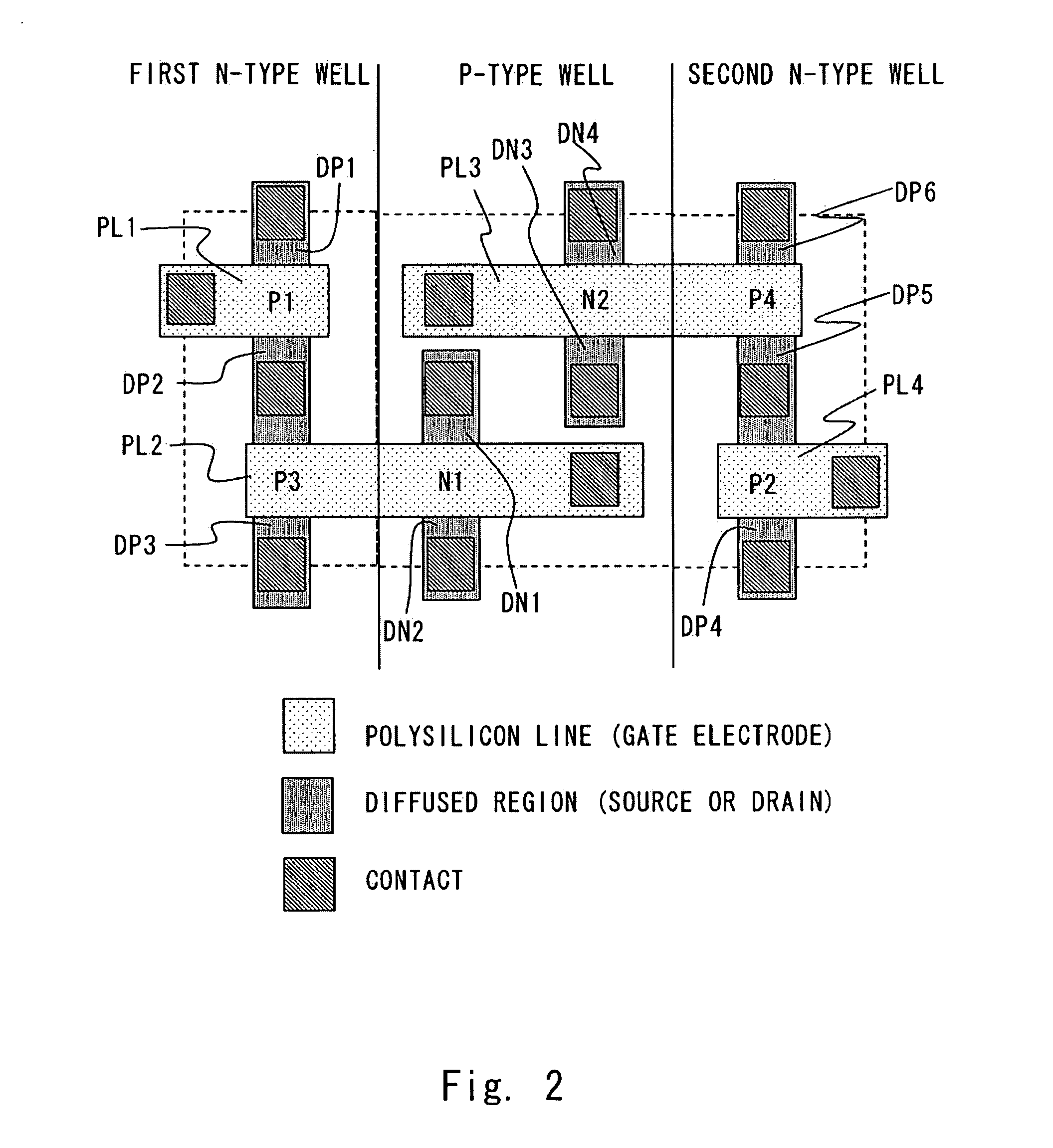
[0023] An embodiment of the present invention is described hereinafter with reference to the drawings. FIG. 1 is a circuit diagram showing a CMOS type SRAM memory cell according to this embodiment. The SRAM memory cell of this embodiment includes NMOS driver transistors N1 and N2, PMOS transfer transistors P1 and P2, and PMOS load transistors P3 and P4.

[0024] The load transistor P3 and the driver transistor N i are connected in series between a power supply Vcc and a ground potential GND. The load transistor P4 and the driver transistor N2 are connected in series between a power supply Vcc and a ground potential GND. The load transistor P4 and the driver trans...


PUM


Abstract

A semiconductor integrated circuit includes a word line extending along a first direction, a first and a second N-well regions, a P-well region disposed between the first and the second N-well regions, a memory cell having a first, second, third, and fourth PMOS transistors, and a first and second NMOS transistors, the first and the second PMOS transistors disposed in the first N-well region along a second direction which is different from the first direction, the first and the second NMOS transistors disposed in the P-well region, and the third and the fourth PMOS transistors disposed in the second N-well region along the second direction.

Description

BACKGROUND OF THE INVENTION [0001] 1. Field of the Invention [0002] The present invention relates to a semiconductor integrated circuit and particularly to a layout of CMOS type SRAM cells. [0003] 2. Description of Related Art [0004] SRAM that configures a memory cell with six transistors can be formed in a standard semiconductor CMOS process and is widely used for system LSI and the like. A conventional SRAM memory cell is comprised of six transistors, which are two NMOS driver transistors, two NMOS transfer transistors and two PMOS load transistors. [0005] Japanese Unexamined Patent Publication No. 2003-115551 (Satomi et al.) discloses a technique to form one each of NMOS driver transistor and NMOS transfer transistor in a first and a second P-well region. It also discloses that two PMOS load transistors are formed in one N-well region. [0006] Meanwhile in recent years as elements become finer, soft error phenomena are reported to occur that causes an inversion of logical data sto...

Claims


Application Information

Patent Timeline
Patent Type & Authority Applications(United States)
IPC IPC(8): G11C11/00
CPCG11C11/412H01L27/1104H10B10/12
Inventor MATSUSHIGE, MUNEAKISATAKE, HIROYUKIFURUTA, HIROSHITAKAHASHI, TOSHIFUMINAKAMURA, HIDEYUKI
Owner RENESAS ELECTRONICS CORP
Learn More