Diamond film-forming silicon and its manufacturing method

a technology of silicon and diamond film, applied in the field of diamond film-forming silicon, can solve the problems of insufficient electrodes

Inactive Publication Date: 2006-09-28
EBARA CORP
View PDF13 Cites 22 Cited by
  • Summary
  • Abstract
  • Description
  • Claims
  • Application Information

AI Technical Summary

Benefits of technology

[0017] The present inventors found that, when electrically conductive diamonds are coated on a silicon substrate with a definite thickness, the foregoing problems can be overcome, and thereby the present invention has been completed.

Problems solved by technology

The wide thermodynamic windows mean that the electrode is inadequate for generating oxygen and hydrogen; however, other reactions can take place at the electrode.

Method used


Image

  • Diamond film-forming silicon and its manufacturing method
  • Diamond film-forming silicon and its manufacturing method
  • Diamond film-forming silicon and its manufacturing method

Examples


Embodiment Construction

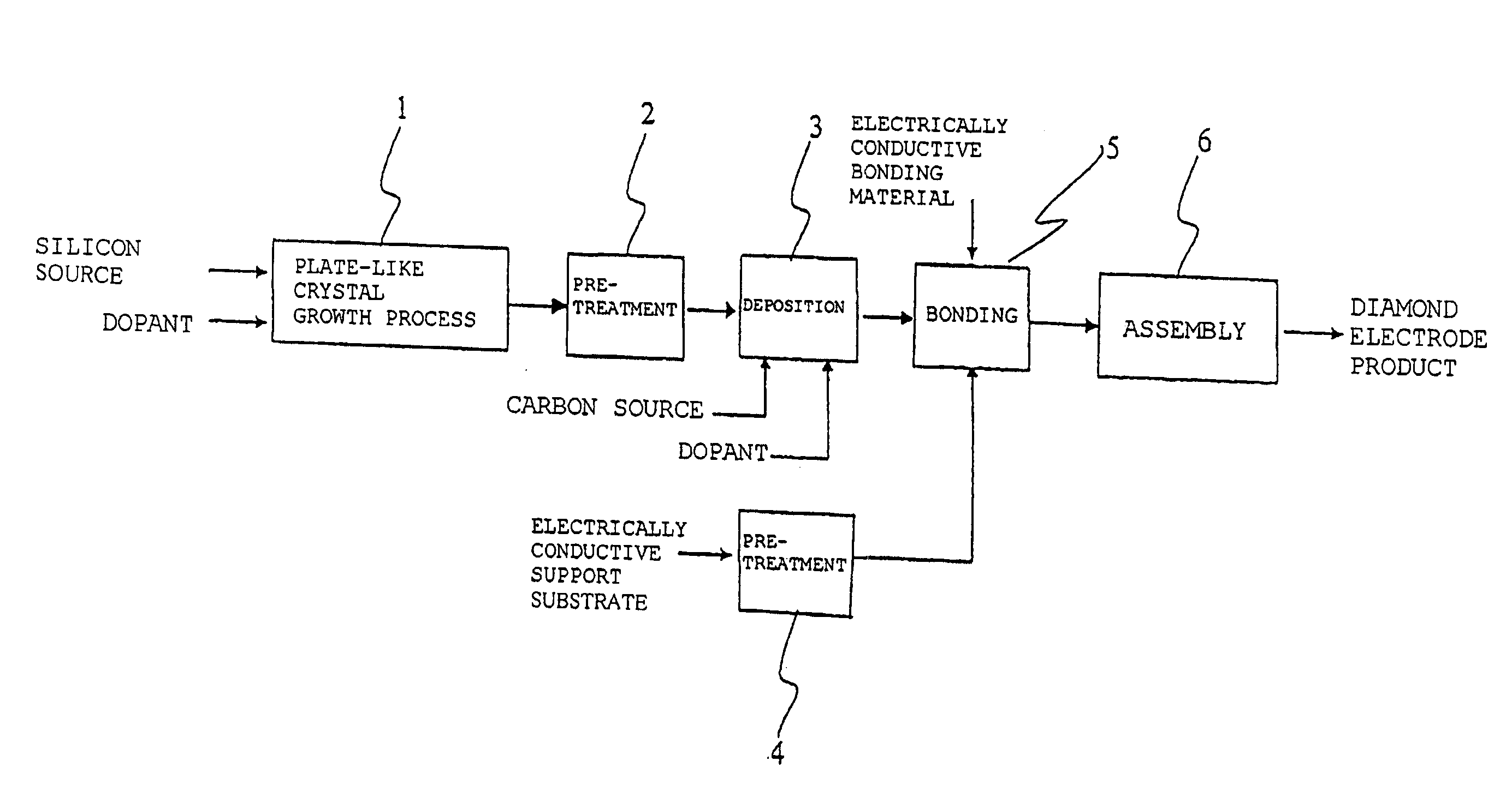
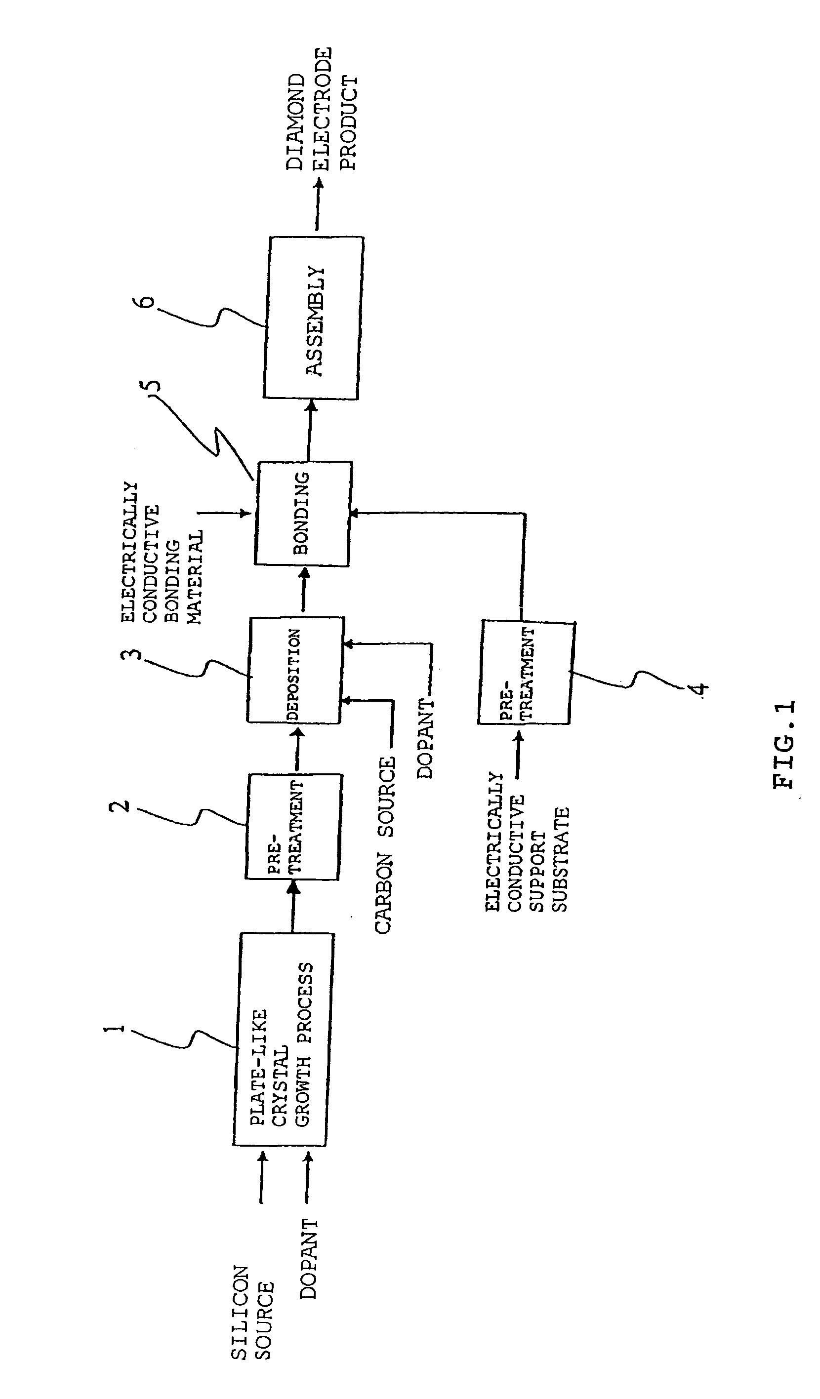
[0029] The plate-like crystal growth process used in the present invention means a process to obtain a plate-like silicon substrate and is not restricted to a particular one as far as it can obtain a silicon substrate having a thickness of 500 μm or less. As specific examples of the plate-like crystal growth processes, the EFG process (Edge-defined Film-fed Growth process), the string ribbon process or the dendritic web process can be preferably cited, and among these the dendritic web process can be cited as a more preferable example. The EFG process is a method to obtain silicon substrate; in which melt silicon is forced to rise by the capillary effects through a slit of a die; that is a mold to feed the melt silicon and to define the crystal shape; followed by pulling up of solidified silicon by bringing into contact with seed crystals. The string ribbon process is another method to obtain the silicon substrate, in which a film supported by the surface tension between several str...


PUM

PropertyMeasurementUnit
thicknessaaaaaaaaaa
binding energyaaaaaaaaaa
lengthaaaaaaaaaa

Abstract

The present invention intends to provide a diamond-coated silicon to be used in an industrially applicable diamond electrode. A diamond-coated silicon comprising a silicon substrate having a thickness of 500 μm or less is coated at least partially with electrically conductive diamond. The silicon substrate having a thickness of 500 μm or less is manufactured by the plate-like crystal growth process, and then the silicon substrate is coated with the electrically conductive diamond by the chemical vapor deposition process to manufacture the diamond-coated silicon. The diamond-coated silicon is flexible and can be stuck to an electrically conductive support substrate, and thereby a large area electrode and a three-dimensional electrode structure can be readily obtained.

Description

TECHNICAL FIELD [0001] The present invention relates to silicon coated with a film of electrically conductive diamond and a manufacturing method thereof. BACKGROUND ART [0002] Diamond has the brilliance characteristic that is utilized in gems and ornaments and is known to be one of the hardest substances on the earth, and exhibits excellent physicochemical stability against frictional wear, chemical, pressure and so on. This physicochemical stability is advantageously used in many familiar products such as diamond cutter for glass, drill tool and grinder disk. [0003] Furthermore, carbon of the diamond belongs to the same group IV of silicon. Accordingly, when carbon forms a diamond structure (sp3 crystal system), exhibits semiconductor characteristics similar to silicon, has strong interatomic binding forces, and has a large band gap such as about 5.5 eV at room temperature corresponding to the binding energy of valence electrons. Similarly to silicon, a p-type semiconductor is form...

Claims


Application Information

Patent Timeline
Patent Type & Authority Applications(United States)
IPC IPC(8): C23C16/00B32B9/00B32B13/04C30B29/06C23C16/27C23C16/54C30B25/02C30B25/18
CPCC23C16/27C23C16/545C30B25/02Y10T428/30C30B25/18C30B29/04C30B29/06
Inventor FUJIMURA, HIROYUKISERIKAWA, ROBERTO MASSAHIROISHIKAWA, NAOKIMISHIMA, TAKAHIRO
Owner EBARA CORP
Why Eureka
Try Eureka