
Layout design method for semiconductor integrated circuit, and semiconductor integrated circuit

a technology of integrated circuits and semiconductors, applied in computer aided design, instruments, solid-state devices, etc., can solve the problems of power supply noise, power supply voltage drop, and excessive voltage supply to transistors, so as to reduce the effect of reducing the influence of power supply noise and voltage drop

Inactive Publication Date: 2006-09-28
RICOH KK
View PDF13 Cites 3 Cited by
  • Summary
  • Abstract
  • Description
  • Claims
  • Application Information

AI Technical Summary

Benefits of technology

[0050] Another advantage of the present invention is the reduction of power supply noise and voltage drop. It is possible to reduce the influences of the power supply noise and voltage drop by using the upper-layer metal efficiently or arranging the bypass capacitor. The power supply noise reduction is also achieved by the capacity between the metal layers by arranging the power supply wiring in the power supply lines and the ground lines alternately.
[0051] Another advantage is the improvement of the planarization and occupancy rate. The uniform formation of metal in the layer of the filler cells can eliminate the problem of the planarization and occupancy rate which arises with the VDSM (very deep submicron) in the recent technique. Moreover, the configuration which meets the design rule is achieved with the configuration state of the filler cells.
[0052] Another advantage is the countermeasure against complicated power supply structure. The power supply wiring is performed by using the filler cells, and it is possible to realize complicated power supply wiring structure. There is no great increase in the man-hour needed, and efficient power supply wiring process can be realized because the arrangement of the filler cells can be incorporated in the conventional layout design method.
[0053] Moreover, the power supply wiring is carried out with the composition which sandwiches the signal lines between the upper and lower layers, the signal wiring can be shielded by the wiring of power supply lines having stable potential, and the cross talk of the signal wiring can be reduced.

Problems solved by technology

The standard cell has the problem in that it requires the external region where the power supply line and the standard cell are mutually connected.
There is the problem that common dimensions of respective macro cells must be used in order to form the power supply lines and grounding lines at the upper and lower edge portions.
As the microscopic process of the semiconductor integrated circuit manufacture progresses, some problems arise and it is demanded to take into consideration the circuit design stage.
The disadvantage of wiring cost and the redundant wiring will take place.
The integration level of the transistors progresses with the development of the microscopic process of the semiconductor integrated circuit manufacture, which results in the problem of power supply noise due to the charging and discharging current at the time of simultaneous switching of the transistors.
Moreover, in the microscopic process, the voltage drop (IR-DROP) in which the voltage supplied to the transistor becomes excessively low arises.
The optimization of the power supply wiring is one of the important issues in the semiconductor integrated circuit design.
However, in the current circumstances, it is difficult to analyze the complicated structure of the power supply wiring, and it is difficult to set up the optimal power supply width.

Method used


Image

  • Layout design method for semiconductor integrated circuit, and semiconductor integrated circuit
  • Layout design method for semiconductor integrated circuit, and semiconductor integrated circuit
  • Layout design method for semiconductor integrated circuit, and semiconductor integrated circuit

Examples


Embodiment Construction

[0075] A description will now be provided of the preferred embodiments of the invention with reference to the accompanying drawings.

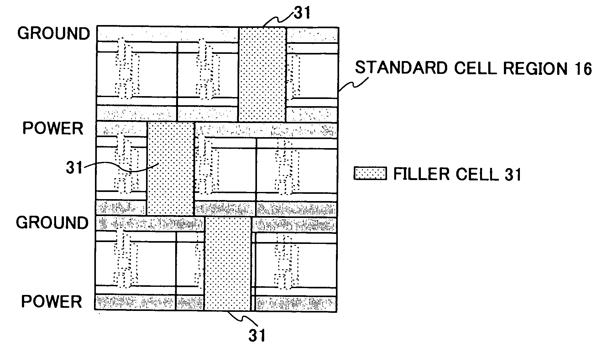
[0076] First, a description will be given of typical examples of filler cells which are used by the layout design method according to the present invention. FIG. 8A and FIG. 8B shows the arrangement of a basic type filler cell 11 used by the layout design method according to the invention. FIG. 9A and FIG. 9B show the arrangement of a substitution type filler cell 12 used by the layout design method according to the invention. FIG. 10A and FIG. 10B show the arrangement of a substitution type filler cell 13 used by the layout design method according to the invention.

[0077] For the sake of convenience of description, the multi-layered semiconductor integrated circuit of one preferred embodiment of the invention is formed into the eight-layer structure. However, the present invention is not limited to this embodiment.

[0078] The basic type filler cell 11...


PUM


Abstract

In a layout design method for a semiconductor integrated circuit, a cell layout library is provided which stores structure information of functional cells and a plurality of groups of filler cells, each filler cell acting to fill space between the functional cells. The functional cells are arranged on a layout based on the structural information from the layout library. The filler cells of any of the plurality of groups are arranged selectively based on the structural information from the layout library so that the filler cells are arranged in channel regions where the functional cells are not located on the layout, each channel region being located at a predetermined distance from signal lines on the layout.

Description

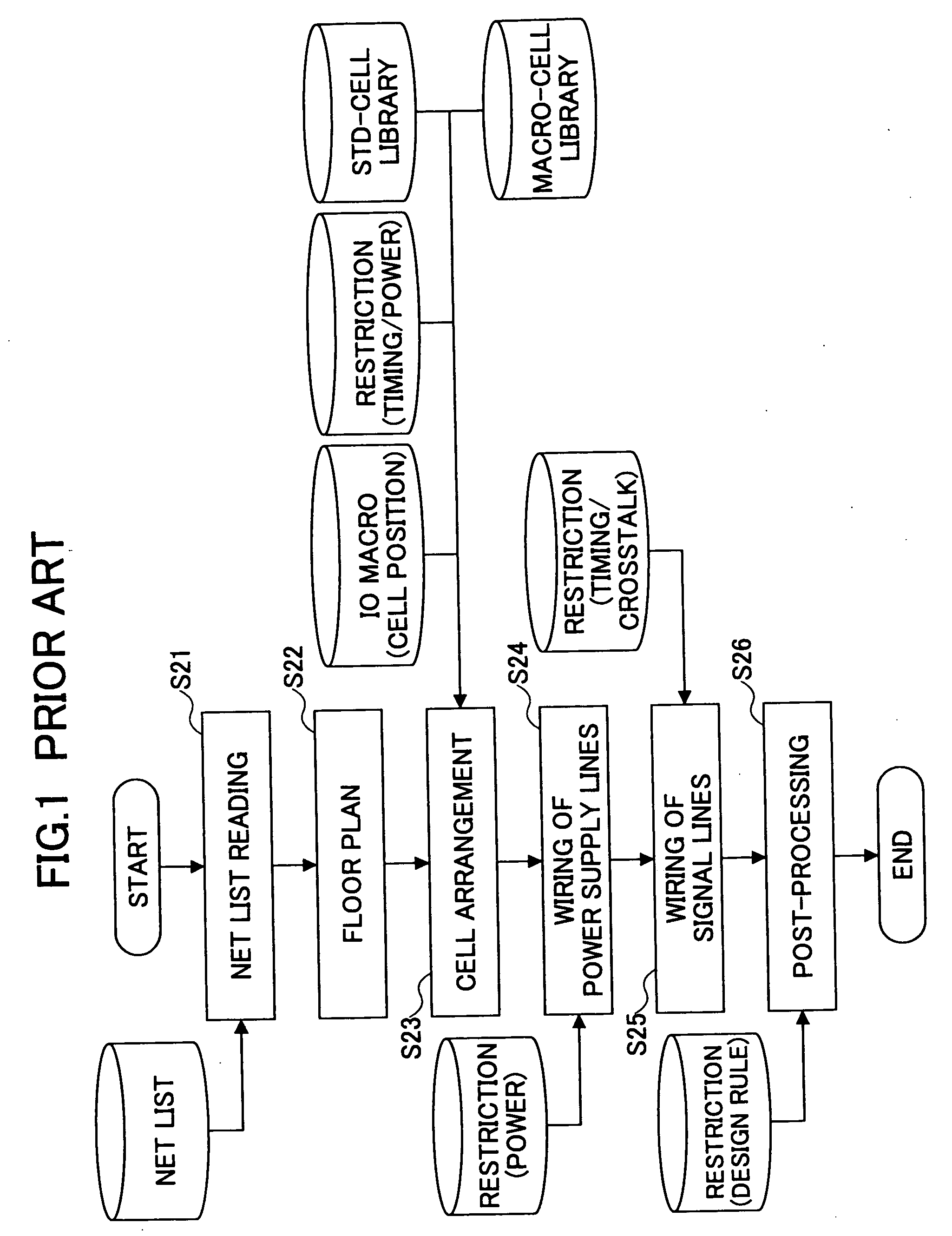
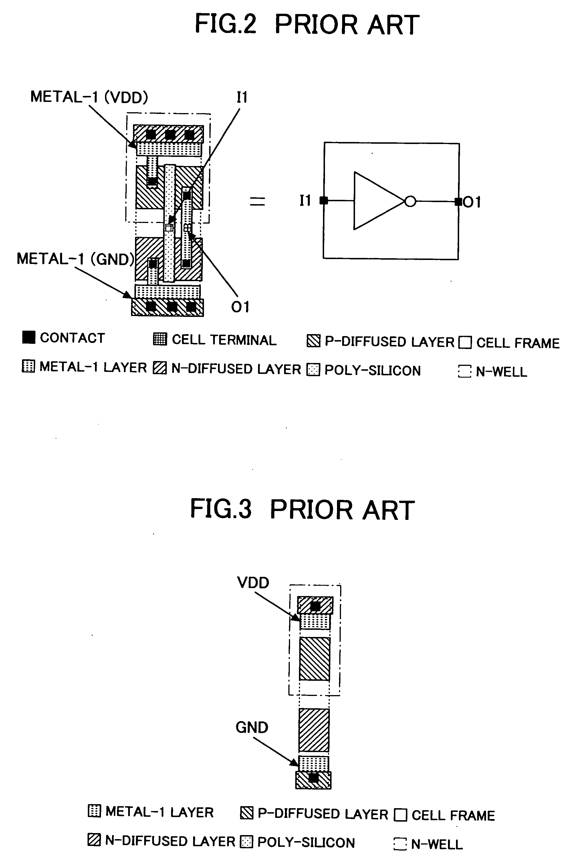
BACKGROUND OF THE INVENTION [0001] 1. Field of the Invention [0002] The present invention relates to a layout design method which creates a multi-layered semiconductor integrated circuit through a cell layout technique, and relates to a semiconductor integrated circuit which is created by the layout design method. [0003] 2. Description of the Related Art [0004] In the layout design of semiconductor integrated circuits, a layout creation tool which is called the automatic placement / wiring tool is used. In the layout creation tool, the structure information of basic cells, such as inverters and NANDs, are registered in the database in advance, the structure information of a desired cell is read from the database and arranged in a predetermined region of a chip layout, so that a semiconductor integrated circuit which meets the given specifications is acquired. [0005]FIG. 1 is a flowchart for explaining a conventional layout design method using the automatic placement / wiring tool. A des...

Claims


Application Information

Patent Timeline
Patent Type & Authority Applications(United States)
IPC IPC(8): G06F17/50H01L21/82H01L21/822H01L27/04
CPCG06F17/5072G06F30/392
Inventor ICHIMIYA, JUNJI
Owner RICOH KK
Learn More