Length measurement pattern, semiconductor device, and method of manufacturing a semiconductor device

a technology of semiconductor devices and measurement patterns, applied in the field of length measurement patterns, semiconductor devices, and methods of manufacturing semiconductor devices, can solve the problems of reducing the yield or inconvenience of properties, weak resistance of subsequent most developed lithography techniques to electron beams, and the use of photoresist in exposure apparatuses, so as to achieve the effect of restrainting the measurement error

Inactive Publication Date: 2006-10-05
RENESAS ELECTRONICS CORP
View PDF2 Cites 0 Cited by
  • Summary
  • Abstract
  • Description
  • Claims
  • Application Information

AI Technical Summary

Benefits of technology

[0016] According to the present invention, the dimension measurement error can be restrained to the minimum by moving the field of view to a region i

Problems solved by technology

When a management of this dimension is neglected, a dimensional abnormality or the like may possibly be generated that directly leads to decrease in the yield or to inconvenience of properties.
However, the photoresist used in an exposure apparatus using an ArF laser light source that is used in the currently most developed process and in the subsequent most developed lithography technique is weak in the resistance to electron beams.
Therefore, it is known that, when electron beams are applied for a long period of ti

Method used


Image

  • Length measurement pattern, semiconductor device, and method of manufacturing a semiconductor device
  • Length measurement pattern, semiconductor device, and method of manufacturing a semiconductor device
  • Length measurement pattern, semiconductor device, and method of manufacturing a semiconductor device

Examples


first embodiment

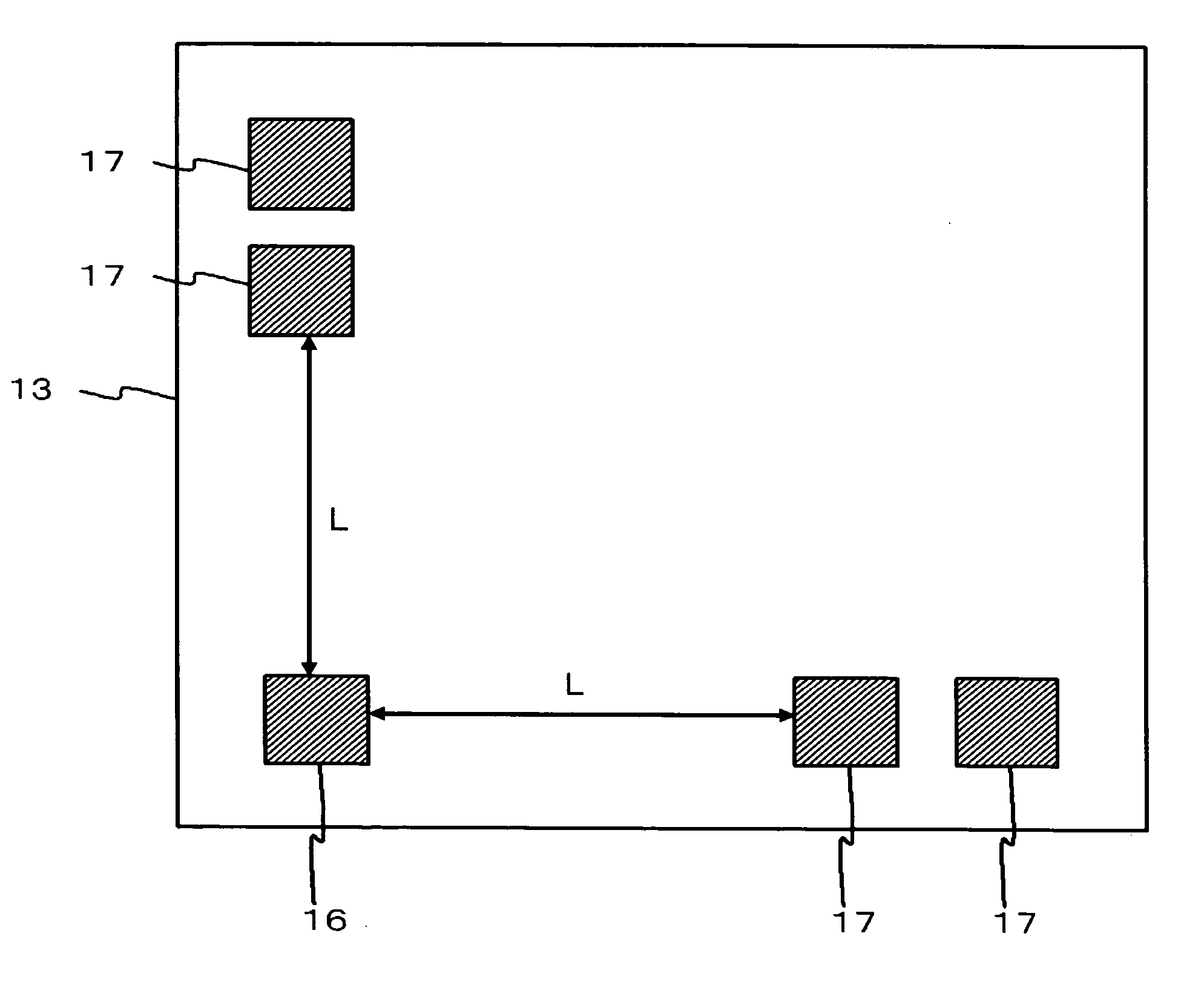
[0025]FIG. 1 shows an example of a dimension measurement pattern of an isolated pattern according to the invention.

[0026] The dimension measurement pattern shown in FIG. 1 is disposed in a resist pattern and is used for the dimension measurement of the resist pattern by the length measurement SEM. Specifically, the length measurement pattern is used in forming a contact and a via on a diffusion layer and on a lower layer interconnect, respectively, with a photoresist.

[0027] This dimension measurement pattern is constructed in the following manner. Namely, a dimension measurement pattern (first pattern) 16 which is an isolated pattern of the via is formed on the lower layer interconnect 13 of the via, and a positioning and focusing pattern (second pattern) 17 for positioning and focusing at the time of length measurement SEM is disposed in the neighborhood of this dimension measurement pattern 16. At this time, the length L between the dimension measurement pattern 16 and the positi...

second embodiment

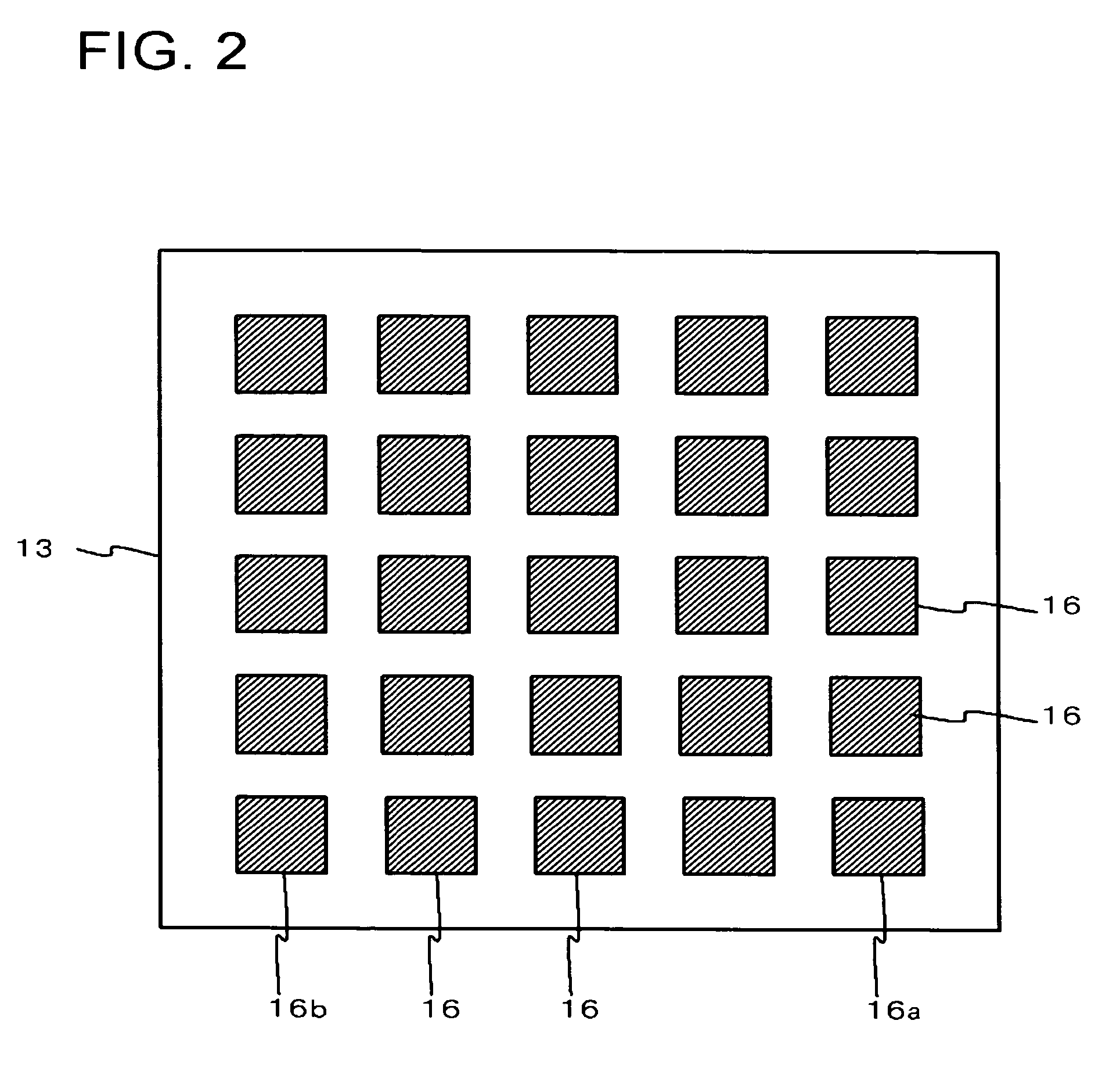
[0034]FIG. 2 shows an example of a dimension measurement pattern of a dense pattern according to the invention. In this example, a dimension measurement pattern 16 of a dense pattern having a sum of 25 patterns (this number is arbitrary) with five patterns in the longitudinal direction and five patterns in the lateral direction is formed in the lower layer interconnect 13.

[0035] Now, assuming that the total size of the dense pattern is twenty or more times as large as the designed value of the via, similar effects can be obtained by performing the positioning and the focusing with a dimension measurement pattern 16a at the right end of the dense pattern shown in FIG. 2 and performing the dimension measurement, for example, with a dimension measurement pattern 16b at the left end after moving the field of view within the same dense pattern. In this example, a part of the dimension measurement pattern 16 of the dense pattern disposed in a lattice form is used as the first pattern, and...


PUM


Abstract

A length measurement pattern is used for forming a contact and a via on a diffusion layer and on a lower layer interconnect, respectively, with a photoresist. The length measurement pattern includes a first pattern 16 serving as an object of length measurement in length measurement SEM and a second pattern 17 disposed to be spaced apart from the first pattern 16 and used for positioning and focusing of the length measurement SEM.

Description

[0001] This application is based on Japanese Patent application NO. 2005-066338, the content of which is incorporated hereinto by reference. BACKGROUND [0002] 1. Technical Field [0003] The present invention relates to a length measurement pattern for dimension measurement in forming a photoresist of a contact or a via on a diffusion layer or on an interconnect, as well as to a semiconductor device using this length measurement pattern and a method of manufacturing a semiconductor device. [0004] 2. Related Art [0005]FIG. 3 is a view of a semiconductor device having a general multiple layer interconnect structure in which a contact 11 is disposed on a diffusion layer 10 which is the lowermost layer; an insulating film 12 is stacked thereon; a lower layer interconnect 13 and a via 14 are formed thereon; and an upper layer interconnect 15 is formed on an upper part of the via 14. In the most developed one of such semiconductor devices, the patterning dimension of the contact 11 and the ...

Claims


Application Information

Patent Timeline
IPC IPC(8): G01N23/00G03F1/00G03F1/70
CPCG01D5/34707G01D5/347G01D2205/90
Inventor OKAMURA, RYUICHI
Owner RENESAS ELECTRONICS CORP
Why Eureka
Try Eureka