Semiconductor element

a technology of semiconductor elements and semiconductors, applied in the field of high-breakdown voltage isolation gate semiconductor devices, can solve problems such as anisotropy in electrical characteristics, and achieve the effect of excellent electrical characteristics and reduced electron mobility

Inactive Publication Date: 2006-10-05
PANASONIC CORP
View PDF7 Cites 31 Cited by
  • Summary
  • Abstract
  • Description
  • Claims
  • Application Information

AI Technical Summary

Benefits of technology

[0049] According to the semiconductor device of the present invention, when the electron mobility reduced due to step-bunching and other unfavorable interface states is improved, this can provide more excellent electrical characteristics than those of a known structure of a semiconductor device.

Problems solved by technology

The step bunches have a height of approximately 50 through 100 nm, leading to anisotropy in electrical characteristics.

Method used


Image

  • Semiconductor element
  • Semiconductor element
  • Semiconductor element

Examples


embodiment 1

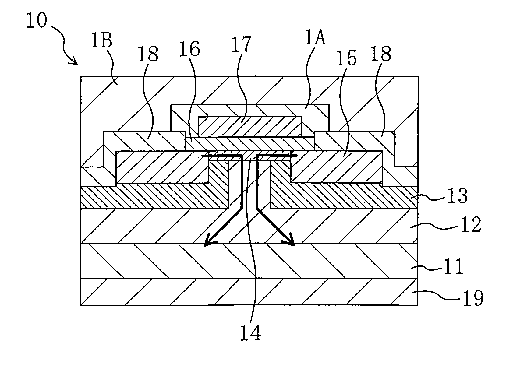
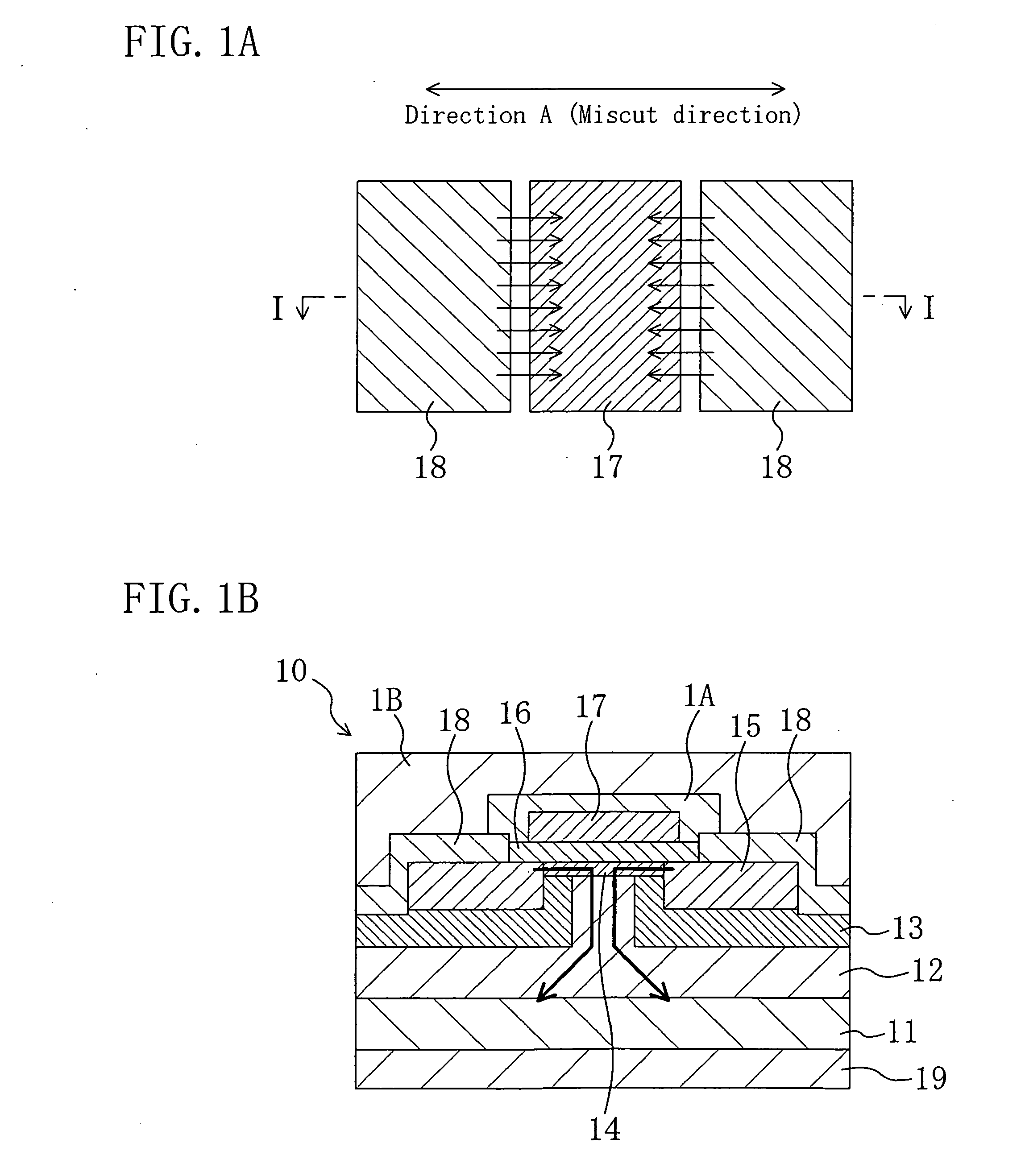
[0104] FIGS. 1(a) and 1(b) are cross-sectional views showing a joint between two unit cells of typical vertical accumulation-mode MOSFETs using a silicon carbide layer in a first embodiment. FIG. 1(a) is a plan view showing some of electrodes of the MOSFETs, and FIG. 1(b) is a cross-sectional view taken along the line I-I in FIG. 1(a).

[0105] As shown in FIGS. 1(a) and 1(b), a semiconductor device of this embodiment has an n+-type 4H—SiC(0001) semiconductor substrate 11. The semiconductor substrate 11 has a surface miscut by approximately 8 degrees in the direction, and its resistivity is approximately 0.02 Ωcm2. An n-type 4H—SiC(0001) silicon carbide layer 12 is formed on the semiconductor substrate 11 to have a thickness of approximately 15 μm and doped with nitrogen at a concentration of 3×1015 cm−3. The n-type silicon carbide layer 12 is formed on the semiconductor substrate 11 by epitaxial growth, and the influence of the semiconductor substrate 11 causes the top surface of th...

embodiment 2

[0149] FIGS. 11(a) and 11(b) are cross-sectional views showing typical lateral accumulation-mode MOSFETs using a silicon carbide layer according to a second embodiment. FIG. 11(a) is a plan view showing some of electrodes of the MOSFETs when seen from above, and FIG. 11(b) is a cross-sectional view taken along the line VII-VII in FIG. 11(a).

[0150] As shown in FIGS. 11(a) and 11(b), a semiconductor device of this embodiment has a semi-insulating 4H—SiC(0001) semiconductor substrate 71. The semiconductor substrate 71 has a surface miscut by approximately 8 degrees in the direction. A 4H—SiC(0001) p-type silicon carbide layer 72 is formed on the semiconductor substrate 71 to have a thickness of approximately 5 μm and doped with aluminum at a concentration of 5×1015 cm−3.

[0151] An n-type channel layer 74 is formed in the middle region of the upper part of the p-type silicon carbide layer 72. In this embodiment, the channel layer 74 is a δ-doped layer obtained by alternately stacking ...


PUM


Abstract

In a semiconductor device of the present invention, the top surface of an n-type silicon carbide layer formed on a silicon carbide substrate is miscut from the (0001) plane in the <11-20> direction. A gate electrode, a source electrode and other elements are arranged such that in a channel region, the dominating current flows along a miscut direction. In the present invention, a gate insulating film is formed and then heat treatment is performed in an atmosphere containing a group-V element. In this way, the interface state density at the interface between the silicon carbide layer and the gate insulating film is reduced. As a result, the electron mobility becomes higher in a miscut direction A than in the direction perpendicular to the miscut direction A.

Description

TECHNICAL FIELD [0001] The present invention relates to a high-breakdown-voltage insulated gate semiconductor device using silicon carbide, and more particularly relates to a MOS field effect transistor (MOSFET) that provides a large-current switching device. BACKGROUND ART [0002] Silicon carbide (SiC) is a semiconductor with a higher hardness and a wider band gap than silicon (Si) and applied to power devices, environmentally resistant devices, high-temperature operating devices, high-frequency devices, and other devices. [0003] For example, MOSFETs as disclosed in Patent Document 1 that will be described below are known as representative switching devices using SiC. FIGS. 14(a) and 14(b) are diagrams showing typical vertical accumulation-mode MOSFETs using SiC. In a unit cell of a typical vertical MOSFET, a source electrode is arranged in the middle of the unit cell. On the other hand, FIGS. 14(a) and 14(b) show the arrangement of electrodes with a gate electrode arranged in the m...

Claims


Application Information

Patent Timeline
Patent Type & Authority Applications(United States)
IPC IPC(8): H01L31/0312H01L21/04H01L29/04H01L29/06H01L29/24H01L29/36H01L29/423H01L29/78
CPCH01L21/049H01L29/045H01L29/0696H01L29/1608H01L29/365H01L29/7838H01L29/4238H01L29/518H01L29/66068H01L29/7802H01L29/41766
Inventor UCHIDA, MASAOKITABATAKE, MAKOTOKUSUMOTO, OSAMUYAMASHITA, KENYATAKAHASHI, KUNIMASAMIYANAGA, RYOKO
Owner PANASONIC CORP
Why Eureka
Try Eureka