Solid-state image pickup element and method of producing the same

a pickup element and solid-state technology, applied in the direction of radio frequency control devices, instruments, television systems, etc., can solve the problems of difficult to form thin metal film on the tapered face with high controllability, difficult to maintain a high sensitivity, and difficult to guide oblique incident light to the photodiode, etc., to achieve the effect of reducing the number of production steps

Active Publication Date: 2006-10-05
FUJIFILM CORP
View PDF0 Cites 27 Cited by
  • Summary
  • Abstract
  • Description
  • Claims
  • Application Information

AI Technical Summary

Benefits of technology

[0050] According to the method, the reflective material portion and the passivation film can be formed in t

Problems solved by technology

Therefore, it is difficult to maintain a high sensitivity.
In this structure, the opening of the optical waveguide is narrow, and therefore it is difficult to guide obliquely incident light to the photodiode.
Therefore, it is difficult to form the thin metal film on the tapered face with high controlla

Method used


Image

  • Solid-state image pickup element and method of producing the same
  • Solid-state image pickup element and method of producing the same
  • Solid-state image pickup element and method of producing the same

Examples


embodiment 1

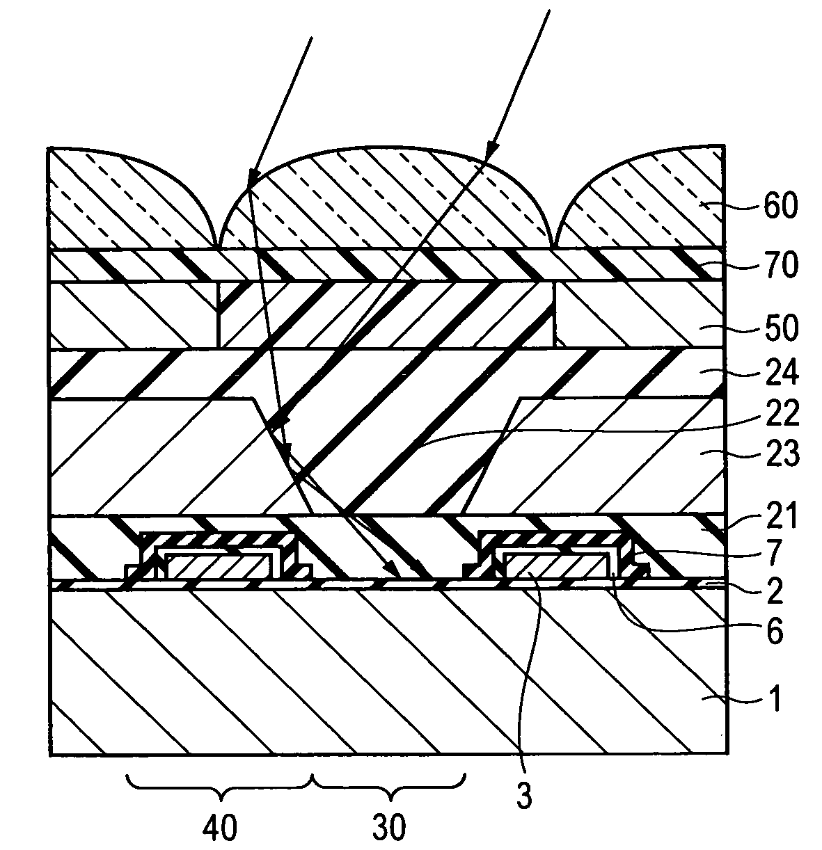
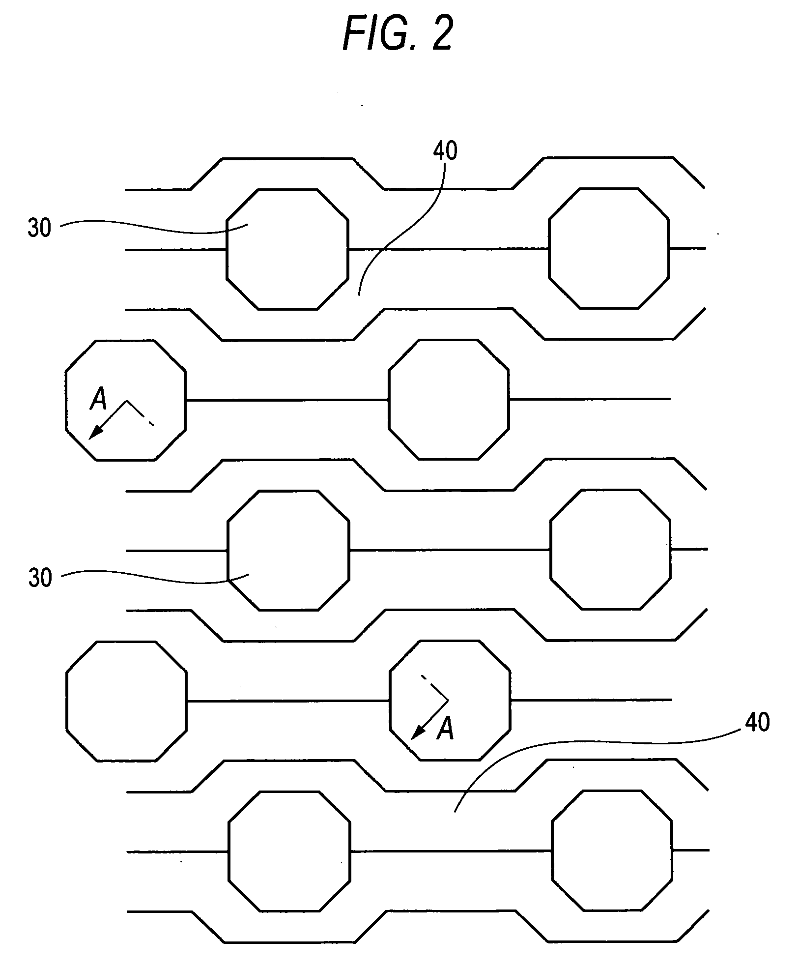
[0067]FIG. 1 is a section view showing a main portion of a solid-state image pickup element, and FIG. 2 is a plan view of a main portion of an imaging region. FIG. 1 is a section view taken along the line A-A of FIG. 2. The solid-state image pickup element is characterized in that an optical waveguide 22 formed above a photodiode 30 serving as a photoelectric converting portion is formed in a reflective material film 23 which covers the surface of a semiconductor substrate, and which has a hole portion on the photodiode 30. The hole portion configures a tapered face that is opened toward an upper portion of the semiconductor substrate, so as to further enhance the light converging property. The reflective material film 23 is configured by a single-layer film of aluminum.

[0068] The reflective material film 23 configured by the aluminum film in which an opening is formed in a region corresponding to the photodiode 30 is disposed above an imaging section of the solid-state image picku...

embodiment 2

[0089] Next, Embodiment 2 of the invention will be described.

[0090] As described in Embodiment 1 above, the embodiment characterized in that the reflective material film 23 is formed in the same step as a wiring layer 23e which is made of an aluminum layer in a peripheral circuit section as shown in FIG. 5.

[0091] The embodiment is generally identical with Embodiment 1. In the embodiment, however, a charge transferring portion and a photodiode are formed in the substrate. The left side of the break line shows the peripheral circuit section, and the right side shows the imaging section.

[0092] The reflective material film 7 which is configured by a tungsten film, and in which an opening is formed in a region corresponding to the photodiode 30 is disposed above the imaging section of the solid-state image pickup element. On the film, the reflective material film 23 which is configured by an aluminum layer, and in which an opening is formed correspondingly with the photodiode 30 is fo...


PUM


Abstract

A solid-state image pickup element comprises: a semiconductor substrate; a photoelectric converting portion formed in the semiconductor substrate; a reflective material portion comprising a hole portion wherein the hole portion is located on a surface, on an area in which the photoelectric converting portion is formed, of the semiconductor substrate, the reflective material portion being formed so as to cover a surface of the semiconductor substrate; and an optical waveguide that propagates incident light while confining the light, to guide the light to the photoelectric converting portion, wherein the optical waveguide is configured by a transparent film formed in the hole portion, the transparent film having a light guiding function.

Description

BACKGROUND OF THE INVENTION [0001] 1. Field of the Invention [0002] The present invention relates to a solid-state image pickup element and a method of producing it, and more particularly to an improvement in characteristics of a solid-state image pickup element having a microstructure. [0003] 2. Description of the Related Art [0004] A solid-state image pickup element using a CCD which is an imaging device such as an area sensor has a basic structure having: a photoelectric converting portion such as a photodiode; a portion for reading a charge from the photoelectric converting portion; and a charge transferring portion comprising charge transfer electrodes for transferring the read charge. The charge transfer electrodes are adjacently arranged on a charge transfer channel formed in the surface of a semiconductor substrate, and sequentially driven by a clock signal. [0005] Recently, in solid-state image pickup elements, the number of imaging pixels is increased, and hence miniaturiz...

Claims


Application Information

Patent Timeline
IPC IPC(8): H01L31/112H01L29/80H01L31/113H04N5/335H01L31/062H04N3/14H01L31/0288
CPCH01L27/1462H01L27/14621H01L27/14627H04N5/335H01L31/0232H04N5/2254H01L27/14685H01L31/02327H04N23/55H04N25/00
Inventor KOORIYAMA, HIDEKI
Owner FUJIFILM CORP
Why Eureka
Try Eureka