Semiconductor device and method for fabricating the same

a semiconductor and semiconductor technology, applied in the direction of semiconductor devices, electrical devices, transistors, etc., can solve the problems of difficult to meet the overlay accuracy required for the impurity diffused layer, the margin for forming patterns cannot meet the requirement of downsizing the device pattern, and the device isolation by sti conducted independently in the peripheral circuit region and the flash memory cell region requires unrealistic step administration, etc., to achieve high accuracy and high accuracy. , the effect of high accuracy

Inactive Publication Date: 2006-10-05
FUJITSU MICROELECTRONICS LTD
View PDF2 Cites 16 Cited by
  • Summary
  • Abstract
  • Description
  • Claims
  • Application Information

AI Technical Summary

Benefits of technology

[0018] According to the present invention, a step is formed in the surface of the semiconductor substrate so that the surface in the first region is lower than the surface in the second region, whereby the height of the upper surface of the first conduction film forming a floating gate can be made substantially the same as the height of the upper surface of the semiconductor substrate in the second region. Thus, the semiconductor substrate in the second region and the first conduction film can be patterned with high accuracy, which makes it possible to provide a semiconductor device including fine memory cells.
[0019] According to the present invention, the step formed in the surface of the semiconductor substrate ensures the flatness of the substrate surface where the conduction film for forming a control gate in the first region and a gate electrode in the second region is to be formed, and the conduction film can be formed flat. Accordingly, the fine control gate can be formed in the first region with high accuracy while the fine gate electrode can be formed in the second region with high accuracy.
[0020] According to the present invention, when the first conduction film forming the floating gate is patterned, the first trench, where the first device isolation region in the first region is formed, is formed by self-alignment, whereby the first trench can be formed without aligning the pattern with high accuracy. Thus, the present invention can facilitate downsizing of memory cells.
[0021] According to the present invention, a sidewall portion of a second conduction film is formed on the side wall of the floating gate, which makes it possible to increase the capacitance between the floating gate and the control gate. According to the present invention, even when the memory cell is further downsized, the capacitance between the floating gate and the control gate can be sufficiently ensured. Thus, according to the present invention, even when the memory cell is downsized, the memory cell can have a required coupling ratio and good electric characteristics.

Problems solved by technology

Accordingly, the device isolation by STI conducted independently in the peripheral circuit region and the flash memory cell region requires unrealistic step administration.
When the times of the thermal processing are increased as in a case, such as the device isolation by STI is conducted independently in the peripheral circuit region and the flash memory cell region, it is difficult to satisfy the overlay accuracy required for the impurity diffused layers.
In this case as well, increasing the margin for forming the patterns cannot meet the requirement of downsizing the device patterns.
Accordingly, it is difficult to ensure the insulation by the device isolation, which is required by a semiconductor device including a flash memory cell.
If the technique described in Reference 1 is applied to the device isolation of a semiconductor device including a flash memory cell, required device characteristics will not be able to be obtained.
In one of the techniques described in Reference 1, thermal processing for forming trenches of different depths is frequently conducted, and the diffusion of the impurities in the well is unavoidable.
Such diffusion of the impurities is a barrier to downsizing the semiconductor device.
However, it will be very difficult to form the fine patterns, based on the up-and-down steps.

Method used


Image

  • Semiconductor device and method for fabricating the same
  • Semiconductor device and method for fabricating the same
  • Semiconductor device and method for fabricating the same

Examples


first embodiment

A First Embodiment

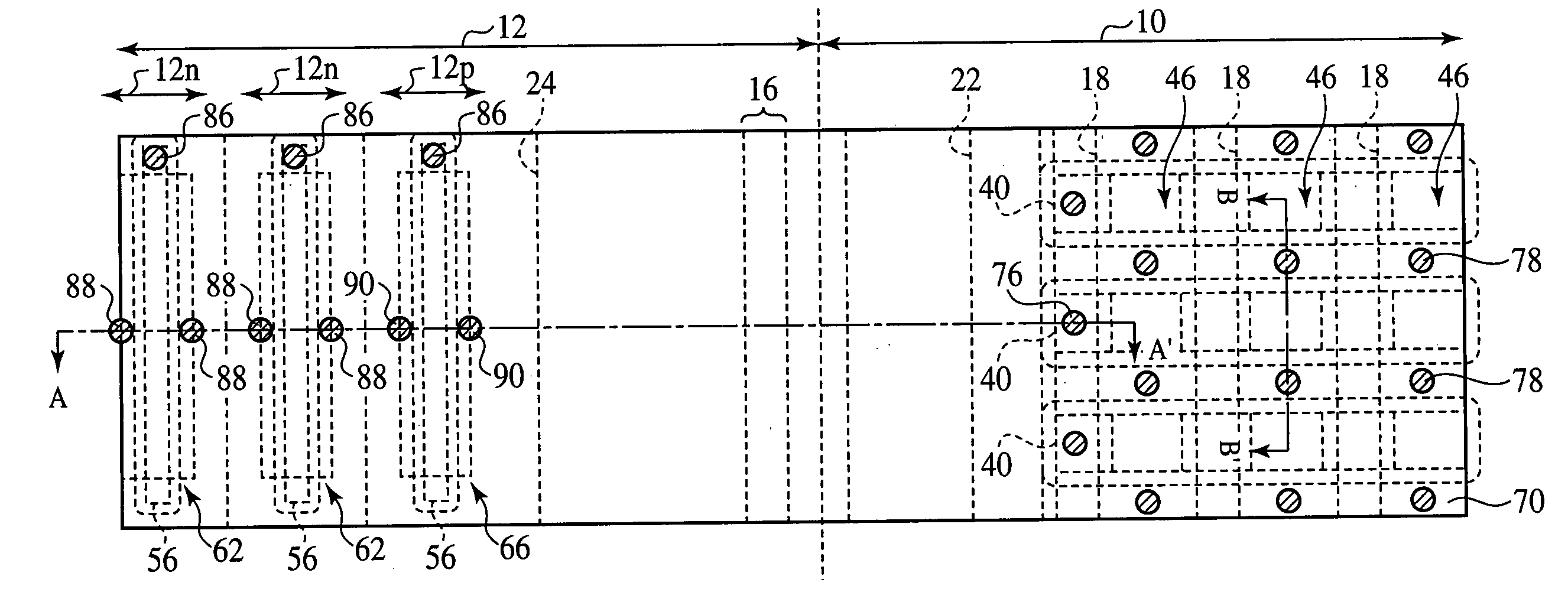
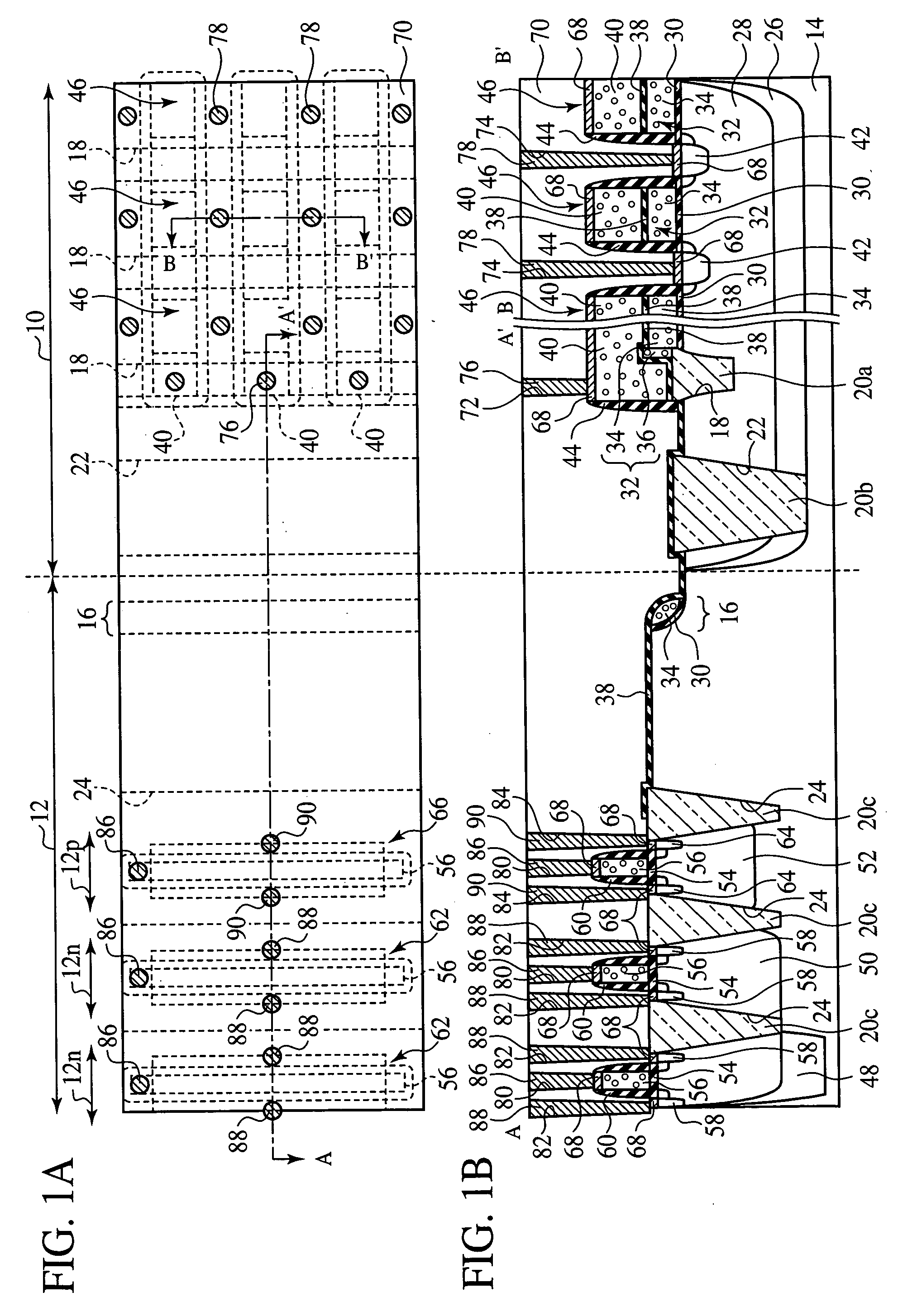
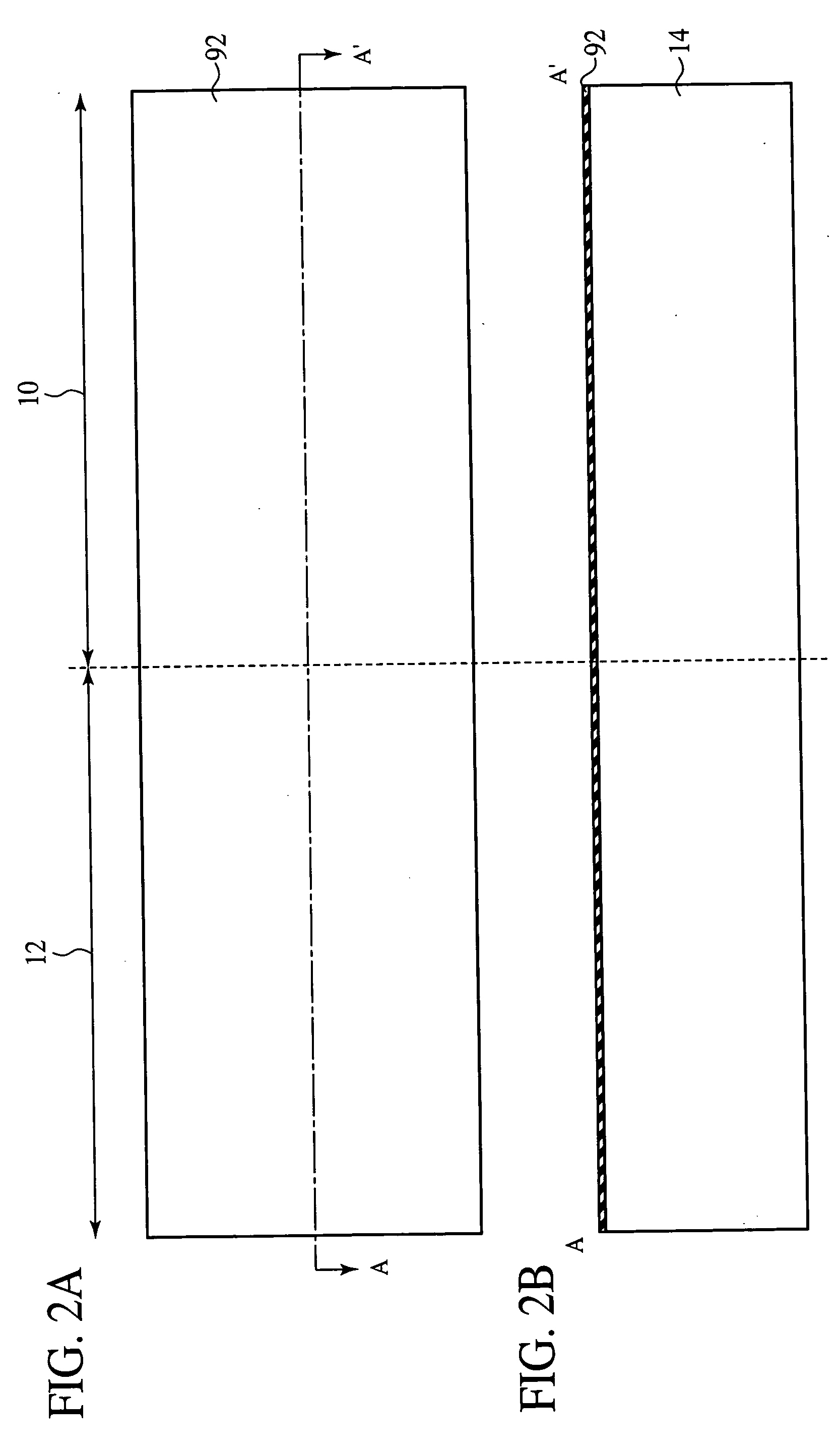
[0028] The semiconductor device and the method for fabricating the same according to a first embodiment of the present invention will be explained with reference to FIGS. 1A to 48. FIGS. 1A and 1B are diagrammatic views of the semiconductor device according to the present embodiment, which illustrate a structure thereof. FIGS. 2A to 41B are diagrammatic views of the semiconductor device according to the present embodiment in the steps of the method for fabricating the same, which illustrate the method. FIGS. 42A to 48 are sectional views of the semiconductor device in the steps of the method for fabricating the same, which illustrate the inconvenience caused when no step is formed in the surface of a silicon substrate.

[0029] First, the structure of the semiconductor device according to the present embodiment will be explained with reference to FIGS. 1A and 1B. FIG. 1A is a plan view of the semiconductor device, which illustrates the structure thereof. FIG. 1B is s...

second embodiment

A Second Embodiment

[0184] The semiconductor device and the method for fabricating the same according to a second embodiment of the present invention will be explained with reference to FIGS. 52A to 59B. FIGS. 52A and 52B are diagrammatic views of the semiconductor device according to the present embodiment, which illustrate a structure thereof. FIGS. 53A to 59B are sectional views of the semiconductor device according to the present embodiment in the steps of the method for fabricating the same, which illustrate the method. The same members of the present embodiment as those of the semiconductor device and the method for fabricating the same according to the first embodiment are represented by the same reference numbers not to repeat or to simplify their explanation.

[0185] First, the structure of the semiconductor device according to the present embodiment will be explained with reference to FIGS. 52A and 52B. FIG. 52A is a plan view of the semiconductor device according to the pre...


PUM


Abstract

The semiconductor device comprises a silicon substrate 14 having a step formed in the surface which makes the surface in a flash memory cell region 10 lower than the surface in a peripheral circuit region 12; a device isolation region 20a formed in a trench 18 in the flash memory cell region 10; a device isolation region 20c formed in a trench 24 deeper than the trench 18 in the peripheral circuit region 12; a flash memory cell 46 including a floating gate 32 and a control gate 40 formed on the device region defined by the device isolation region 20a; and transistors 62, 66 formed on the device regions defined by the device isolation region 20c.

Description

CROSS-REFERENCE TO RELATED APPLICATIONS [0001] This application is based upon and claims the benefit of priority from the prior Japanese Patent Application No. 2005-105507, filed on Mar. 31, 2005 and the prior Japanese Patent Application No. 2005-222119, filed on Jul. 29, 2005, the entire contents of which are incorporated herein by reference. BACKGROUND OF THE INVENTION [0002] The present invention relates to a semiconductor device and a method for fabricating the same, more specifically a semiconductor device including a nonvolatile memory and a method for fabricating the same. [0003] In a semiconductor device including a nonvolatile memory, in addition to flash memory cells, high-voltage transistors for controlling the flash memory, and low-voltage transistors for a high-performance logic circuit are integrated on one semiconductor chip. The flash memory cell has a gate electrode of the stacked structure of a control gate and a floating gate laid the one on the other, which is di...

Claims


Application Information

Patent Timeline
Patent Type & Authority Applications(United States)
IPC IPC(8): H01L29/788
CPCH01L27/105H01L27/11543H01L27/11526H01L27/115H10B41/40H10B69/00H10B41/48
Inventor OGURA, JUSUKE
Owner FUJITSU MICROELECTRONICS LTD
Why Eureka
Try Eureka