

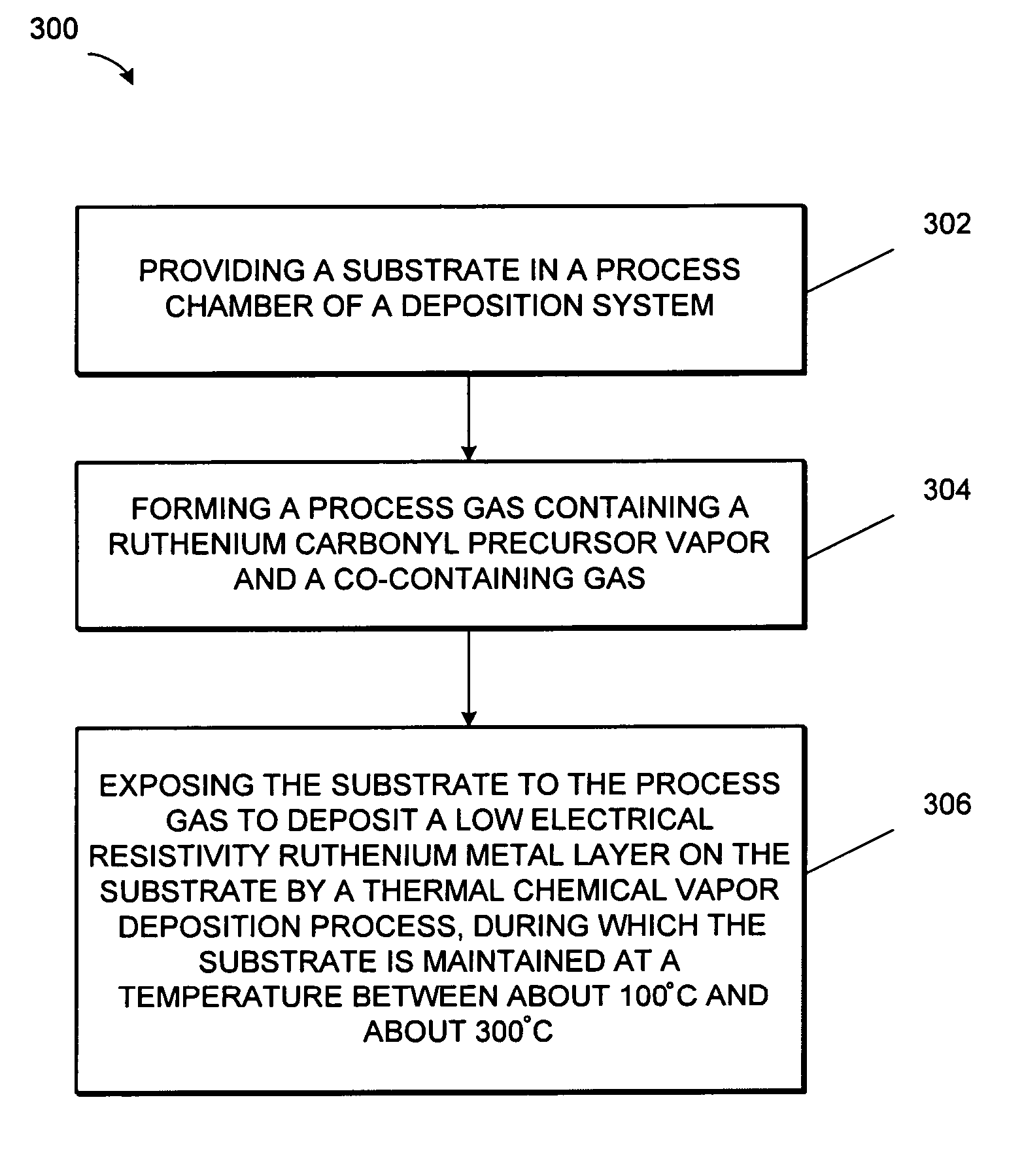
Low-temperature chemical vapor deposition of low-resistivity ruthenium layers
a ruthenium layer, low-resistance technology, applied in chemical vapor deposition coatings, basic electric elements, coatings, etc., can solve the problems of poor material properties of ruthenium deposition layers that are deposited by tcvd, poor ruthenium deposition rate, high electrical resistivity, etc., to achieve low electrical resistivity and low electrical resistivity
- Summary
- Abstract
- Description
- Claims
- Application Information
AI Technical Summary
Benefits of technology
Problems solved by technology
Method used
Image

Examples
Embodiment Construction
[0017] In the following description, in order to facilitate a thorough understanding of the invention and for purposes of explanation and not limitation, specific details are set forth, such as a particular geometry of the deposition system and descriptions of various components. However, it should be understood that the invention may be practiced in other embodiments that depart from these specific details.
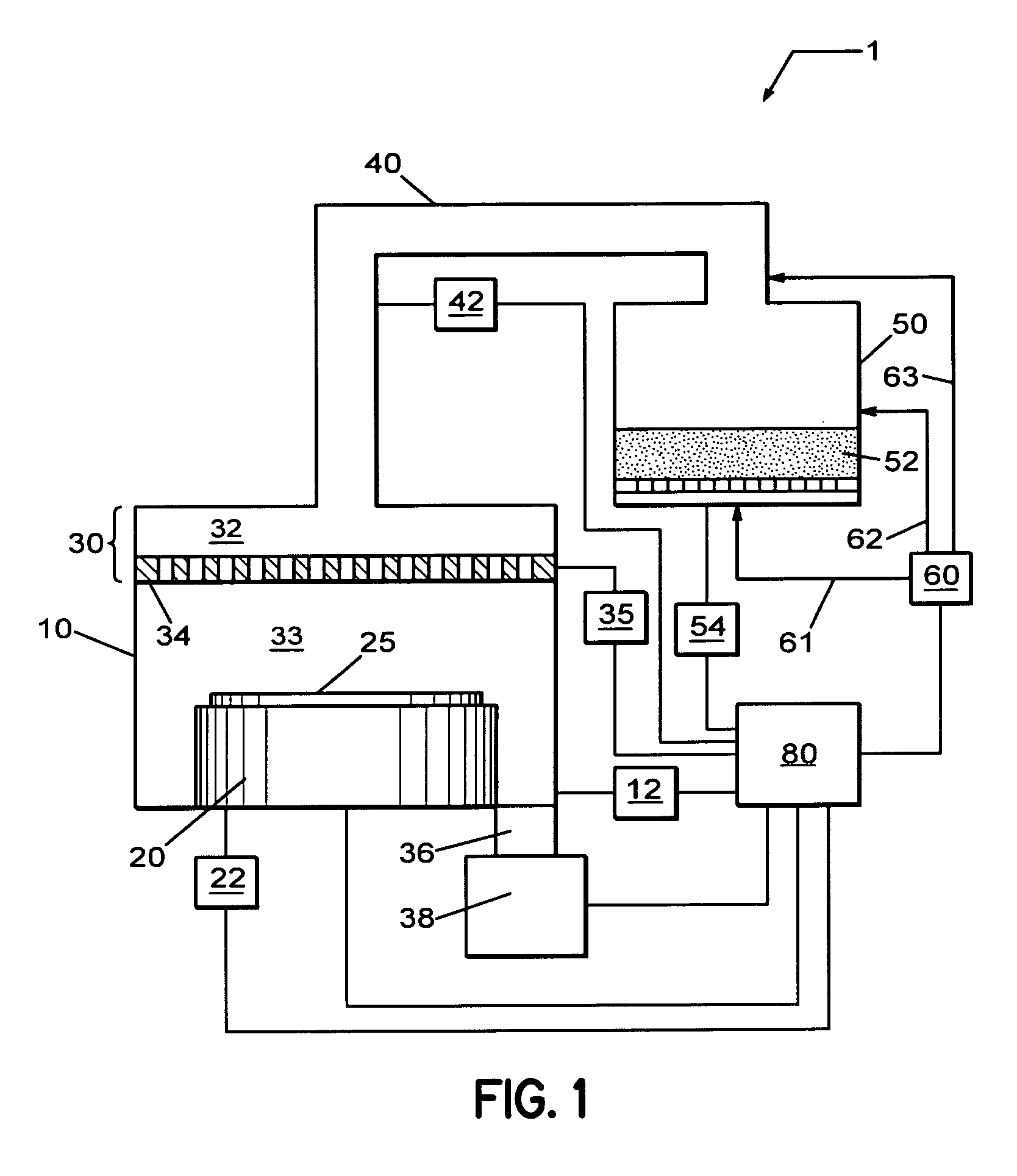
[0018] Referring now to the drawings, wherein like reference numerals designate identical or corresponding parts throughout the several views, FIG. 1 illustrates a deposition system 1 for depositing a ruthenium metal layer on a substrate from a ruthenium carbonyl precursor according to one embodiment of the invention. The deposition system 1 comprises a process chamber 10 having a substrate holder 20 configured to support a substrate 25 upon which the ruthenium metal layer is formed. The process chamber 10 is coupled to a metal precursor vaporization system 50 via a vapor precur...
PUM
| Property | Measurement | Unit |
|---|---|---|
| temperature | aaaaa | aaaaa |
| temperature | aaaaa | aaaaa |
| temperature | aaaaa | aaaaa |
Abstract
Description
Claims
Application Information