Photoresist mask/smoothing layer ensuring the field homogeneity and better step-coverage in OLED displays

a technology of photoresist and mask, applied in the direction of discharge tube luminescnet screen, discharge tube/lamp details, electric discharge lamps, etc., can solve the problems of device failure in individual pixels or segments, device breakage, and large short circuit in the device, and achieve the effect of simplifying the slop

Inactive Publication Date: 2006-10-05
NAT RES COUNCIL OF CANADA
View PDF4 Cites 4 Cited by
  • Summary
  • Abstract
  • Description
  • Claims
  • Application Information

AI Technical Summary

Benefits of technology

[0014] In one embodiment the invention provides a photoresist-based smoothing mask technique to overcome the difficulties encountered in the prior art in the fabrication of OLEDs. The use of a photoresist as a smoothing layer permits direct patterning of the OLEDs and simplified sloping by temperature reflow.
[0017] A particularly convenient class of material to use for the smoothing layer is photosensitive resins. Such resins have several advantages. They can be used in spin coating and therefore provide a conformal coating smoothing out all edges. They can be directly patterned by lithography (exposure and development) without pattern transfer, thereby providing a simple process. They reflow during a hard-bake, which in this case stabilizes the photoresist and provides a smooth pixel edge. They are of a similar nature to the active materials of the OLEDs and therefore will be protected by any passivation layers that are applied to ensure the integrity of the OLEDs.
[0018] The invention thus relates to a technique which can use commercially available photoresist as a masking / smoothing layer to define the emissive and non-emissive areas of the light emitting devices. Typical thickness of this layer is in the 0.2-2 micrometer range, that is thick enough to cover all the steps produced after ITO etching. During the baking process, the photoresist reflows, providing a tapered slope at the edge . This photoresist layer therefore not only functions as a mask layer to define an active area but also blunts the steep edges produced by ITO patterning and provides tapered edges to maintain continuity in the cathode layer so that the device can be connected to the outside world. Subsequently, organic layers and a metal cathode are applied to complete the process. In this way, short circuits and discontinuities in cathode can be substantially avoided.

Problems solved by technology

This will cause the device to break down.
This will cause massive short circuits in the devices.
This type of discontinuity will cause device failure in OLEDs based on a common cathode (or common anode) design and may also cause device failure in individual pixels or segments due to the open circuit between the electrode layer and connection pads.
This process is complicated.
The deposition of dielectric material is also expensive.
Various solutions have been proposed in the prior art, all of which are unsatisfactory for one reason or another.

Method used


Image

  • Photoresist mask/smoothing layer ensuring the field homogeneity and better step-coverage in OLED displays
  • Photoresist mask/smoothing layer ensuring the field homogeneity and better step-coverage in OLED displays
  • Photoresist mask/smoothing layer ensuring the field homogeneity and better step-coverage in OLED displays

Examples


Embodiment Construction

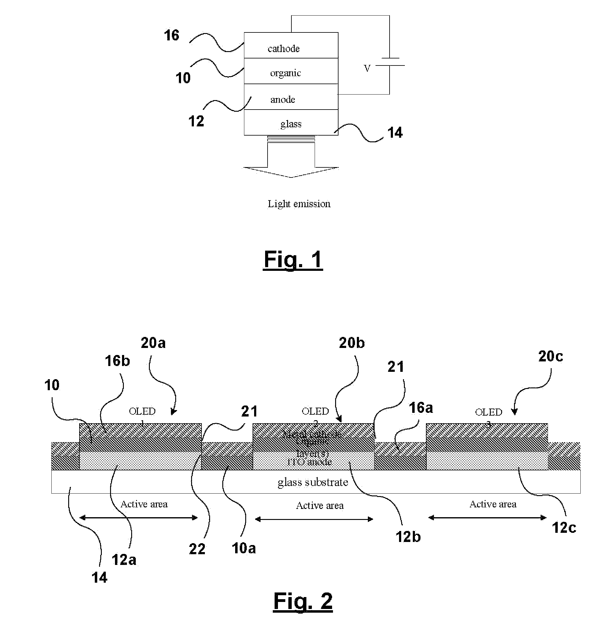
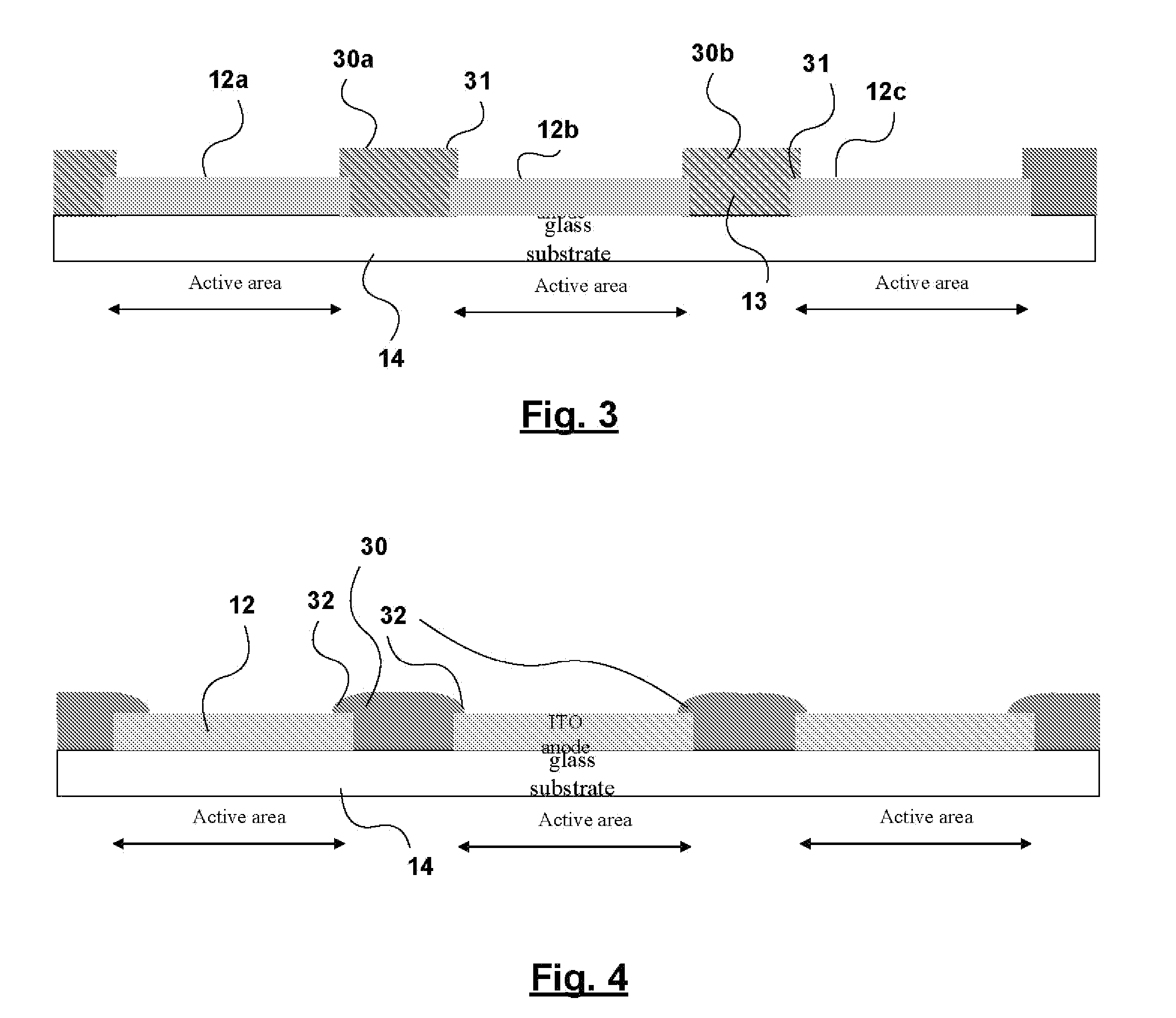
[0026] A method of making an OLED in accordance with one embodiment of the invention will now be described with reference FIGS. 3 and 4. An ITO coated glass substrate 14 is cleaned in a conventional manner. The ITO layer 12 is then patterned and etched to produce individual anodes 12a, 12b, 12c. It will be appreciated that other suitable transparent materials can be employed for the substrate.

[0027] A layer of commercial photoresist 30 approximately 0.2˜2 μm thick is applied between the individual anodes. This layer is exposed and developed to leave the individual columns 30a, 30b of photoresist protruding between the individual anodes and overhanging slightly over the step edges 31 of the anodes 12.

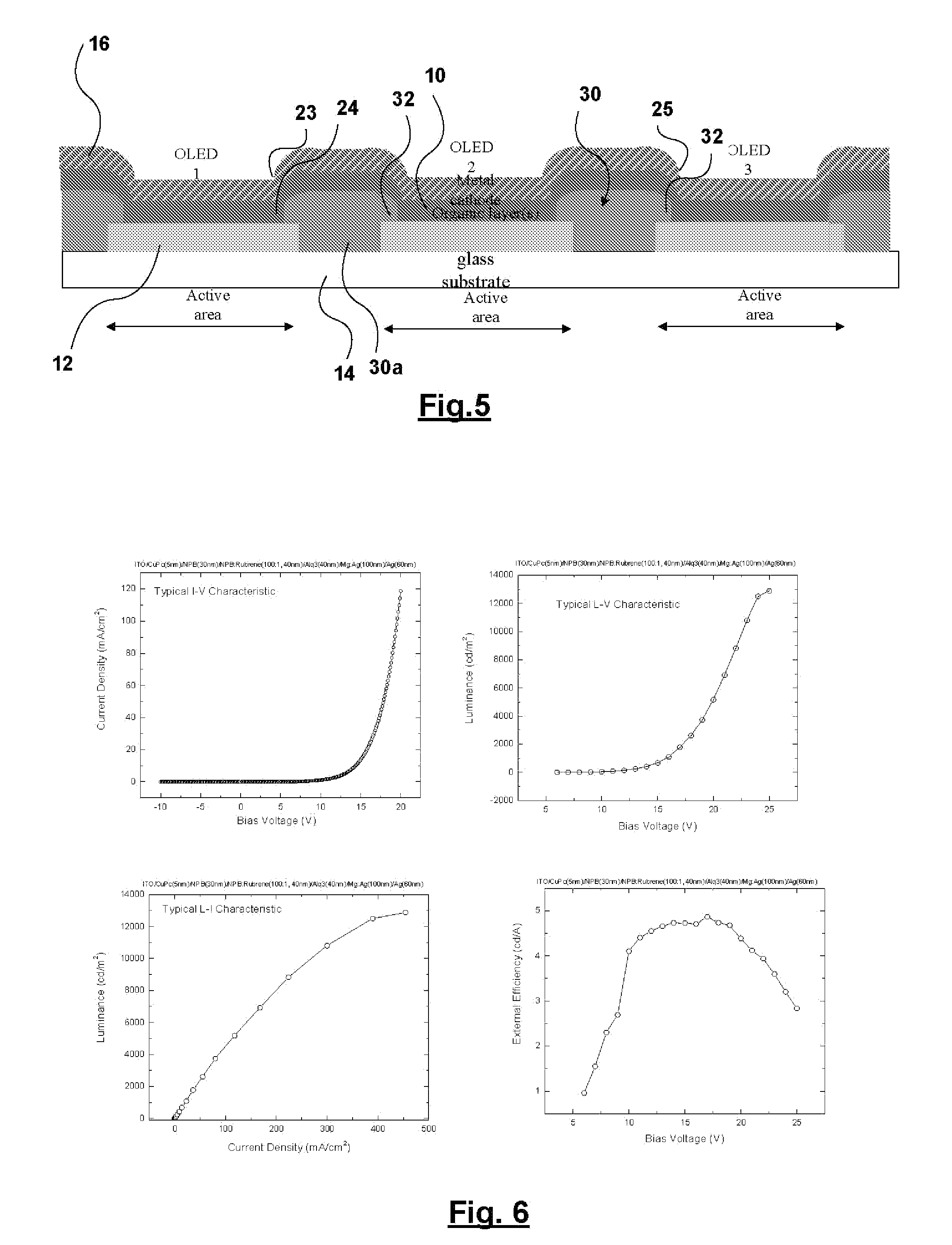
[0028] The wafer is then subjected to a baking step in which the photoresist reflows to produce columns with tapered edges 32 overhanging the exposed portions of the individual anodes as shown in FIG. 4.

[0029] The photoresist layer acts as a mask for the subsequent deposition by therm...


PUM


Abstract

A method of making an organic light emitting device (OLED) is disclosed wherein an inert insulating conformal smoothing layer is deposited over a protruding structure. The smoothing layer is patterned to expose portions of the structure underlying the smoothing layer and defining active regions of the device. The inert smoothing layer is treated, preferably by heat reflow, to taper the layer over the stepped edges of the structure on the exposed portions. Additional layers are then deposited over the smoothing layer and the exposed portions of the structure. The smoothing layer blunts all underlying layer edges and provides sloped edges wherever a step occurs from one layer to another. This effect results in a homogeneous field across the pixel and the continuity in the layers deposited after the photoresist layer.

Description

CROSS REFERENCE TO RELATED APPLICATION [0001] This application is a divisional application of copending U.S. application Ser. No. 10 / 638,493 and claims the benefit under 35 USC 119(e) of prior provisional application Ser. No. 60 / 402,540 filed Aug. 12, 2002.FIELD OF INVENTION [0002] The invention relates to the field of optical devices, and in particular to organic light emitting devices (OLEDs), and to a method of manufacturing such devices. BACKGROUND OF INVENTION [0003] OLEDs have recently shown promise for use as a light source in optical displays. A typical structure for an OLED is shown in FIG. 1 and consists of a stack of organic semiconductor layers 10 between a transparent electrode 12 (usually an indium tin oxide (ITO) layer acting as an anode) on a glass substrate 14 and another electrode 16 (usually a layer of low work function metal, metal alloy or cermet material acting as a cathode). At positive bias, electric current will flow through the device and light emission wil...

Claims


Application Information

Patent Timeline
Patent Type & Authority Applications(United States)
IPC IPC(8): H01L51/52H05B33/02H01L27/32H01L51/00H01L51/30H01L51/56H05B33/14H05B33/20H05B33/22
CPCH01L27/3283H01L51/0052H01L51/0059H01L51/0078H05B33/22H01L51/56H05B33/14H05B33/20H01L51/0081H10K59/173H10K85/615H10K85/311H10K85/631H10K85/324H10K71/40H10K71/00
Inventor TAO, YE
Owner NAT RES COUNCIL OF CANADA
Why Eureka
Try Eureka