Pattern defect inspection method and apparatus using image correction technique

a technology of image correction and pattern defect, applied in the field of pattern defect inspection methods and apparatuses using image correction techniques, can solve the problems of pattern defect in lithography, increased manufacturing costs, and lower production yield, and achieve the effect of increasing accuracy

Inactive Publication Date: 2006-10-05
ADVANCED MASK INSPECTION TECH
View PDF6 Cites 11 Cited by
  • Summary
  • Abstract
  • Description
  • Claims
  • Application Information

AI Technical Summary

Benefits of technology

[0014] According to the invention, it is possible to provide high-reliability pattern defect inspection methodology capable of performing position correction with increased accuracy.

Problems solved by technology

Yield advancement is inevitable for fabrication of large-scale integrated (LSI) circuit devices, which require increased manufacturing costs.
One of factors which lower production yield is the presence of pattern defects in lithography-use photomasks, which are typically used when transferring an ultrafine circuit pattern onto semiconductor wafers.
Unfortunately, this method requires consumption of an increased length of exploring time if the step-like movements or shifts are lessened in the minimum unit thereof and thus is encountered with a problem as to limits in attainable accuracy.
Another problem in the prior art is an increase in apparatus manufacturing costs occurring due to increases in total amount of arithmetical computation required.

Method used


Image

  • Pattern defect inspection method and apparatus using image correction technique
  • Pattern defect inspection method and apparatus using image correction technique
  • Pattern defect inspection method and apparatus using image correction technique

Examples


first embodiment

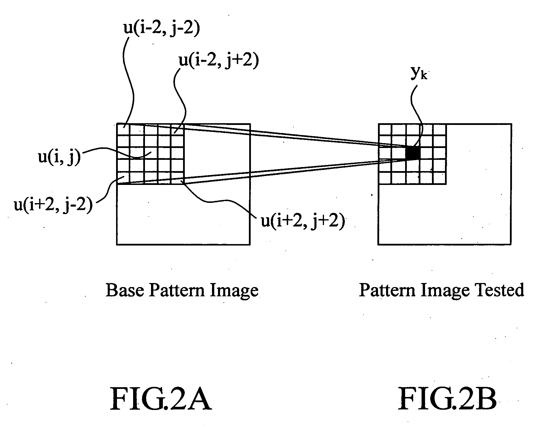
[0019] An explanation will be given of an embodiment which is arranged to develop an inspection-use fiducial or “base” pattern image from a database of design data of this pattern and compare it to the sensed pattern image of a workpiece being tested, thereby inspecting the workpiece for defects. FIG. 3 shows schematically a configuration of mask defect inspection apparatus suitable for use in this embodiment as will be described in detail below.

[0020] The mask defect inspection apparatus of FIG. 3 is generally made up of an arithmetic computation control unit 300 including a host computer as its major component, and an observational data generating unit 310 operable to sense an optical image of the circuit pattern of a workpiece—here, photomask.

[0021] The computation control unit 300 includes a host computer 301, a signal transmission path 302 which has a bundle of address and data buses connected to the host computer 301, a stage control circuit 303 coupled to the signal transfe...

second embodiment

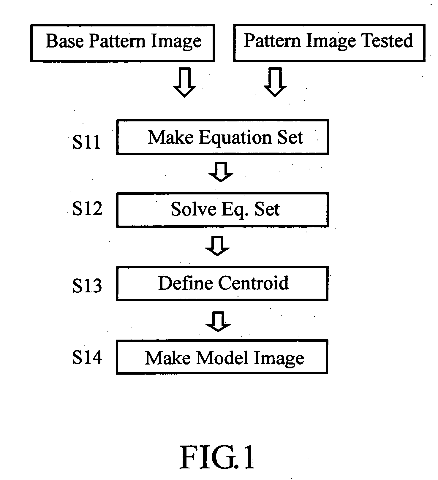
[0048] A second embodiment of the invention is drawn to a pattern inspection method employing the image correction method of the first embodiment stated supra. More specifically, execution of a sequence of the process steps S11 to S14 of FIG. 1 results in creation of a new version of inspection fiducial pattern image with its image shifts being accurately corrected. This new fiducial pattern image is then compared to a pattern image to be tested, thereby enabling inspection of defects in the circuit pattern formed on a workpiece.

[0049] A technique used in this process may be any one of currently established schemes which employ algorithms for inspection of coincidence between a couple of arbitrary images. An example of such algorithms is a level comparison algorithm which specifies at every portion a difference in gradation between a fiducial pattern and a to-be-tested pattern and, if a portion with its gradation difference being in excess of a predefined value is found, then deter...
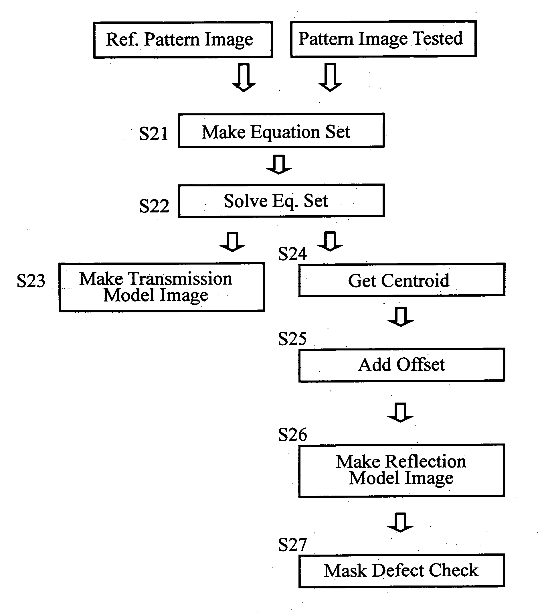
third embodiment

[0050] A third embodiment of the invention relates to a defect inspection method adaptable for use in the case of testing a photomask pattern by using both of a pattern obtained by transmission light and a pattern obtained by reflection light. Although a mask defect inspection apparatus employable in this embodiment will be described below, repetitive explanations are eliminated as for the same process and system configuration as those of the first and second embodiments stated supra.

[0051] See FIG. 4, which depicts a configuration of main part of the mask defect inspection apparatus adaptable for use in this embodiment. The illustrative apparatus is generally made up of an arithmetic computation control unit 400 including a host computer as its main component, and an observational data generator unit 410 which operates to pick up the pattern image of a workpiece being tested, e.g., a photomask.

[0052] The main controller 400 includes a host computer 401, a signal transfer path 402...


PUM

PropertyMeasurementUnit
optical imageaaaaaaaaaa
optical imagesaaaaaaaaaa
reflectionaaaaaaaaaa

Abstract

An image correction method employable in a pattern inspection method for emitting light falling onto a workpiece with a pattern formed thereon and for inspecting a pattern image resulting from the pickup of an optical image of the workpiece by comparing it to a corresponding fiducial pattern image is disclosed. The method includes the step of generating a system of equations describing therein an input/output relation using a 2D linear prediction model(s) with respect to the pattern image being tested and the fiducial pattern image. Then, estimate the equation system by least-squares methods to thereby obtain a parameter of the equation system. Next obtain a centroid of the parameter. Then perform interpolation using the value of the centroid, thereby to generate a corrected image. A pattern defect inspection method using the image correction method is also disclosed.

Description

CROSS-REFERENCE TO RELATED APPLICATION(S) [0001] This application is based on and claims priority of Japanese Patent Application (JPA) No. 2005-095464, filed on Mar. 29, 2005, the disclosure of which is incorporated herein by reference. FIELD OF THE INVENTION [0002] The present invention relates generally to pattern inspection techniques for inspecting an object for pattern defects and, more particularly, to a pattern defect inspection method of checking defects of a lithography mask employable in the manufacture of semiconductor devices and liquid crystal display (LCD) panels. This invention related to an image correction apparatus. This invention also relates to an image correction method adaptable for use in the pattern inspection method. DESCRIPTION OF RELATED ART [0003] Yield advancement is inevitable for fabrication of large-scale integrated (LSI) circuit devices, which require increased manufacturing costs. One of factors which lower production yield is the presence of patter...

Claims


Application Information

Patent Timeline
Patent Type & Authority Applications(United States)
IPC IPC(8): G06K9/00G01B11/30G01N21/956G03F1/72G03F1/84G06T1/00G06T7/60H01L21/027
CPCG03F1/84G06T2207/30148G06T7/004G06T7/001G06T7/70
Inventor SUGIHARA, SHINJIOAKI, JUNJI
Owner ADVANCED MASK INSPECTION TECH
Why Eureka
Try Eureka