Method of producing highly strained pecvd silicon nitride thin films at low temperature

a technology of silicon nitride and high-temperature process, which is applied in the direction of coatings, semiconductor devices, chemical vapor deposition coatings, etc., can solve the problems that certain elements of silicon-based transistors, silicide contacts and highly-activated dopants can be undesiredly affected by high-temperature processes, and achieve the effect of increasing the stress

Inactive Publication Date: 2006-10-05
GLOBALFOUNDRIES INC
View PDF22 Cites 86 Cited by
  • Summary
  • Abstract
  • Description
  • Claims
  • Application Information

AI Technical Summary

Benefits of technology

[0021] The inventive method is a departure from the prior art because it is directed towards preserving the mechanical strain state of the deposited film, while increasing its st

Problems solved by technology

For example, certain III-V compound semiconductors such as, for example, GaAs, are not stable above 500° C. In addition, certain elements of silicon-based transistors (e.g., the silicide contacts and the highly-activated dopants) can be undesirably affected by high-temperature processes.
State of the art CMOS devices have relatively low middle-of-the-line (MOL) temperature budget, which is gradually approaching the back-end-of-the-line (BEOL) temperatures

Method used


Image

  • Method of producing highly strained pecvd silicon nitride thin films at low temperature
  • Method of producing highly strained pecvd silicon nitride thin films at low temperature
  • Method of producing highly strained pecvd silicon nitride thin films at low temperature

Examples


Embodiment Construction

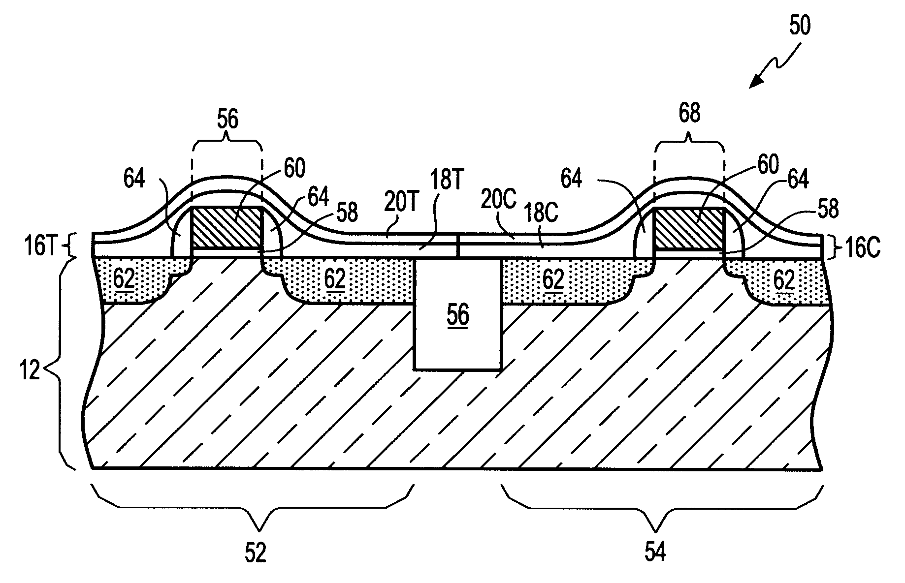
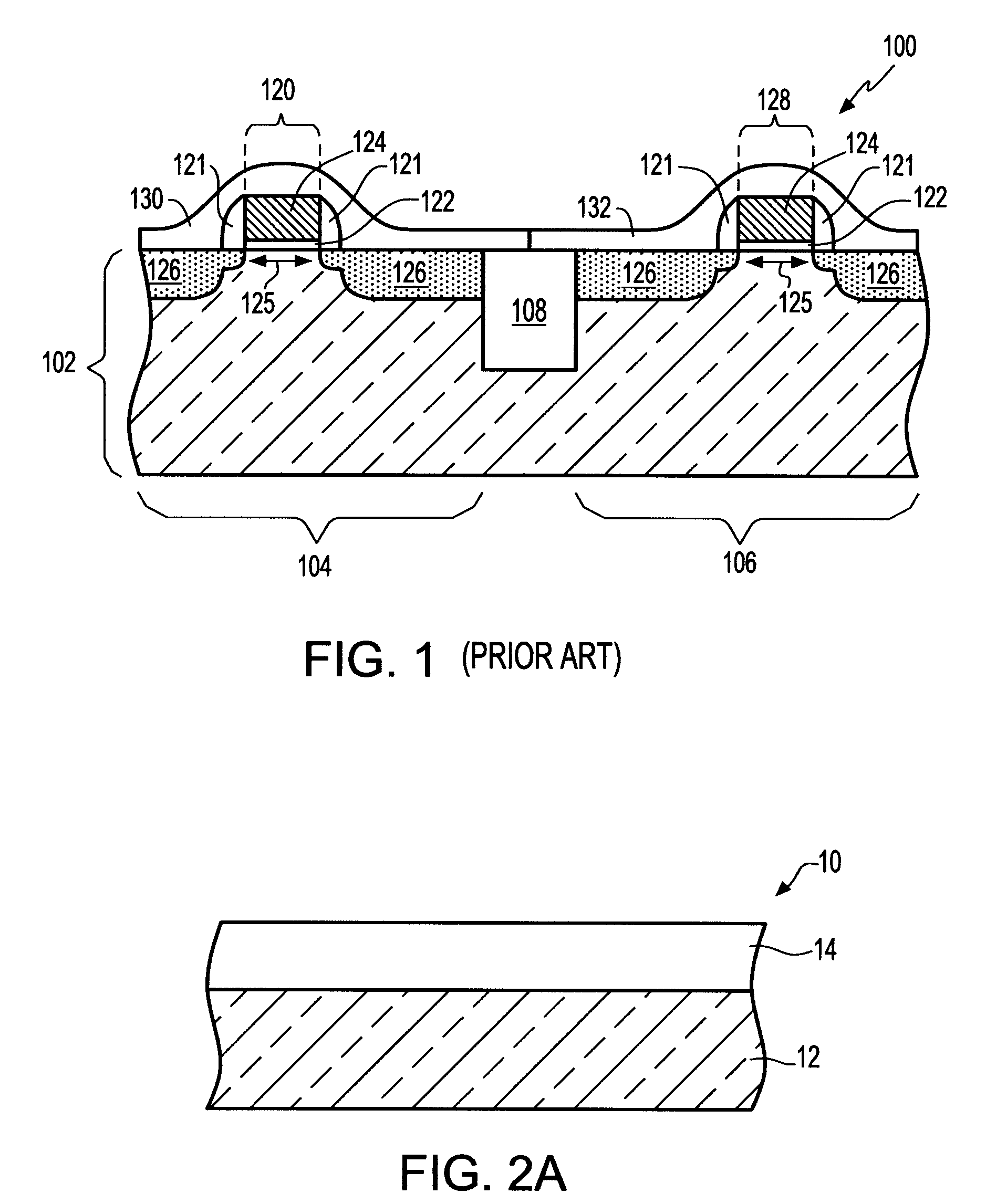
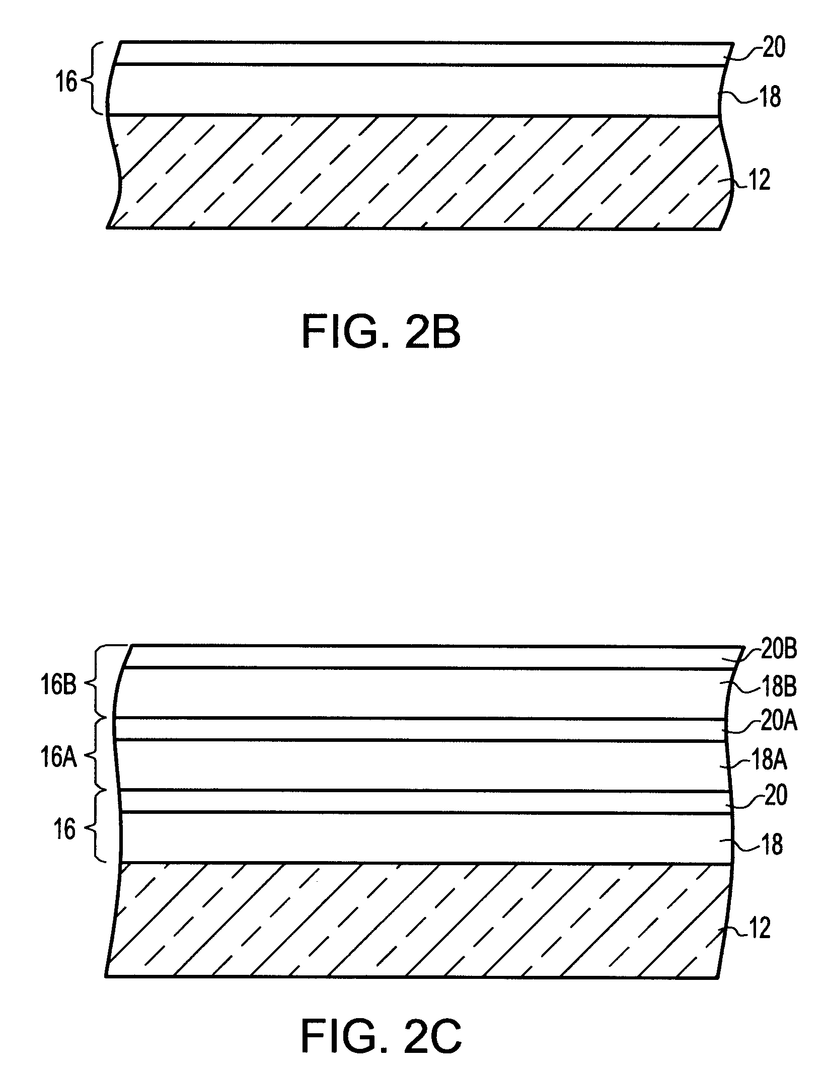
[0026] The present invention, which provides a method of increasing the level of stress for an amorphous thin film stressor material by a technique in which the internal structure of the film is modified, will now be described in greater detail by referring to the following discussion and drawings that accompany the present application. It is noted that the drawings of the present application are provided for illustrative purposes and thus they are not drawn to scale.

[0027] Reference is made to FIGS. 2A-2C which illustrates the basic processing steps of the present invention. Specifically, FIG. 2A illustrates a structure 10 that includes an amorphous thin film stressor material 14 that is formed atop a surface of a semiconductor substrate 12. It is observed that FIGS. 2A-2C illustrate only a small portion of the semiconductor substrate 12 and that the inventive method can be used over the entire surface of the semiconductor substrate 12 which can include transistor devices, such as...


PUM

PropertyMeasurementUnit
Temperatureaaaaaaaaaa
Timeaaaaaaaaaa
Thicknessaaaaaaaaaa

Abstract

A method for increasing the level of stress for amorphous thin film stressors by means of modifying the internal structure of such stressors is provided. The method includes first forming a first portion of an amorphous film stressor material on at least a surface of a substrate, said first portion having a first state of mechanical strain defining a first stress value. After the forming step, the first portion of the amorphous film stressor material is densified such that the first state of mechanical strain is not substantially altered, while increasing the first stress value. In some embodiments, the steps of forming and densifying are repeated any number of times to obtain a preselected and desired thickness for the stressor.

Description

FIELD OF THE INVENTION [0001] The present invention relates to semiconductor device manufacturing, and more particularly to a method for increasing the level of stress of an amorphous thin film stressor, i.e., stress inducing, material. BACKGROUND OF THE INVENTION [0002] Stress engineering plays an important role in increasing the performance of semiconductor devices. Typical examples of such application of stress are widely used strained semiconductor lasers and strained transistors (e.g., strained-channel field effect transistors, FETs) and related strained circuits such as complementary metal oxide semiconductor (CMOS) circuits. In the case of strained FET channels, the stress is applied to the transistor structure in such a way that the device channel region is beneficially strained causing increased mobility of electrons (or holes), which in turn gives a substantial improvement in device speed. The positive effect of crystal lattice strain onto electron and hole mobility depend...

Claims


Application Information

Patent Timeline
IPC IPC(8): H01L21/265H01L21/31
CPCC23C16/345C23C16/45523H01L21/3185H01L29/7843H01L21/823864H01L29/7833H01L21/823807H01L21/02274H01L21/02271H01L21/0217
Inventor BELYANSKY, MICHAEL P.GLUSCHENKOV, OLEGLI, YINGMALLIKARJUNAN, ANUPAMA
Owner GLOBALFOUNDRIES INC
Why Eureka
Try Eureka