Method of fabricating semiconductor devices and method of adjusting lattice distance in device channel

Inactive Publication Date: 2006-10-12
UNITED MICROELECTRONICS CORP
View PDF6 Cites 10 Cited by
  • Summary
  • Abstract
  • Description
  • Claims
  • Application Information

AI Technical Summary

Benefits of technology

[0012] Accordingly, the present invention is directed to a method of fabricating a semiconductor device to improve device performance.
[0013] The present invention is also directed to a method of adjusting a lattice distance of a device channel region to enhance electron mobility in the channel region.
[0019] The SAB layer of the present invention creates a tension stress which will change the lattice distance in the channel region of the substrate under the gate structure. Accordingly, the electron mobility in the channel region of the substrate under the gate structure is improved. The device performance is also improved. In addition, according to the present invention, a semiconductor process is conducted while the lattice distance is adjusted without additional processes and costs.
[0023] The lattice adjusting layer of the present invention creates a tension stress during the thermal process so that the tension stress changes the lattice distance of the channel region. Accordingly, the electron mobility in the channel region is improved and the device performance is also enhanced.

Problems solved by technology

Because the adhesion of most metals to silicon is unsatisfactory, currently, the material of the gate electrode is polysilicon.
The application of a polysilicon gate electrode, however, incurs other issues.
For example, the device performance decays due to the high resistance of the polysilicon.
However, when the size of the device shrinks, the lattice distance in the channel region 128 seriously affects the electron mobility.

Method used


Image

  • Method of fabricating semiconductor devices and method of adjusting lattice distance in device channel
  • Method of fabricating semiconductor devices and method of adjusting lattice distance in device channel
  • Method of fabricating semiconductor devices and method of adjusting lattice distance in device channel

Examples


Embodiment Construction

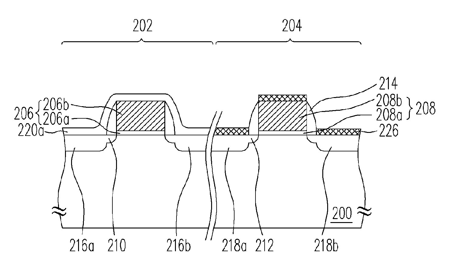
[0027]FIGS. 2A-2F are schematic cross sectional views showing the progression of a method of fabricating a semiconductor device according to a preferred embodiment of the present invention. Referring to FIG. 2A, a substrate 200 is provided. The substrate 200 includes, for example, a device area 202 and a peripheral circuit area 204. Gate structures 206 and 208 are formed over the substrate 200 of the device area 202 and the peripheral circuit area 204, respectively, wherein, the gate structure 206 can be a portion of a memory device or an electro-static discharge (ESD) protection circuit. The gate structure 206 includes the gate dielectric layer 206a and the gate electrode layer 206b. The gate structure 208 can be a portion of a logic device. The gate structure 208 includes the gate dielectric layer 208a and the gate electrode layer 208b. In addition, the material of the gate dielectric layers 206a and 208a can be, for example, silicon oxide. The material of the gate electrode layer...


PUM


Abstract

A method of fabricating semiconductor devices is provided. A plurality of gate structures is formed over a substrate. A source region and a drain region are formed in the substrate and adjacent to sidewalls of each gate structure. A self-aligned salicide block (SAB) layer is formed over the substrate to cover the gate structures and the exposed surface of the substrate. An anneal process is performed. The SAB layer creates a tension stress during the anneal process so that the substrate under the gate structures is subjected to the tension stress. A portion of the SAB layer is removed to expose a portion of the gate structures and a portion of the surface of the substrate. A salicide process is performed.

Description

BACKGROUND OF THE INVENTION [0001] 1. Field of the Invention [0002] The present invention relates to a semiconductor process, and more particularly to a method of fabricating a semiconductor device and a method of adjusting a lattice distance in the device channel region. [0003] 2. Description of the Related Art [0004] In the early days, a metal-oxide-semiconductor (MOS) device is composed of a metal gate electrode, a gate dielectric layer, and a semiconductor substrate. Because the adhesion of most metals to silicon is unsatisfactory, currently, the material of the gate electrode is polysilicon. The application of a polysilicon gate electrode, however, incurs other issues. For example, the device performance decays due to the high resistance of the polysilicon. Accordingly, with the present technology, after forming the device, a salicide process is performed to form metal silicide on the gate electrode and the source / drain regions to reduce the resistance of the device. [0005] In ...

Claims


Application Information

Patent Timeline
IPC IPC(8): H01L21/8234H01L21/336
CPCH01L21/823412H01L21/823418H01L21/823443H01L29/7845H01L29/7833H01L29/7843H01L29/665Y10S438/938
Inventor LIU, ALEXHUANG, CHENG-TUNGSHIAU, WEI-TSUNLIAO, KUAN-YANG
Owner UNITED MICROELECTRONICS CORP
Why Eureka
Try Eureka