Method of manufacturing thin film transistor and method of manufacturing liquid crystal display device using the same

Active Publication Date: 2008-06-12
LG DISPLAY CO LTD
View PDF4 Cites 8 Cited by
  • Summary
  • Abstract
  • Description
  • Claims
  • Application Information

AI Technical Summary

Benefits of technology

[0013]An advantage of the present invention is to provide a method of manufacturing a thin film transistor capable of reducing a manufacturing time, and a method of manufacturing a liquid crystal display device using the same.
[0014]Another advantage of the present invention is to provide a method of manufacturing a thin film transistor capable of improving electron mobility.

Problems solved by technology

However, due to the lack of technology for arranging the nanomaterial until now, there is a limitation in manufacturing a nano thin film transistor.
Accordingly, it takes quite a manufacturing time to arrange the nanomaterial.
Thus, technology for easily arranging the nanomaterial is urgently needed.
However, it is extremely difficult to form the nanowire with directionality through a present technological level.

Method used


Image

  • Method of manufacturing thin film transistor and method of manufacturing liquid crystal display device using the same
  • Method of manufacturing thin film transistor and method of manufacturing liquid crystal display device using the same
  • Method of manufacturing thin film transistor and method of manufacturing liquid crystal display device using the same

Examples


first embodiment

[0025]FIGS. 1A to 1H are views of manufacturing processes of a thin film transistor according to a

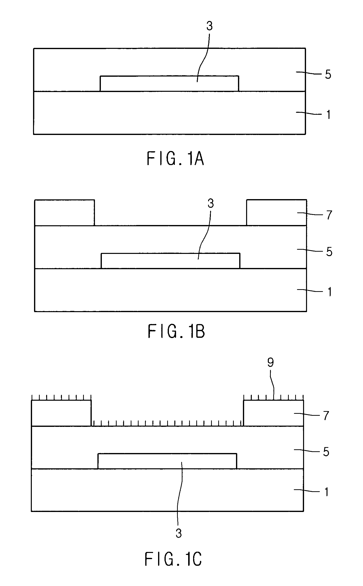
[0026]As illustrated in FIG. 1A, a first metal layer is deposited on a substrate 1, and then patterned to form a gate electrode 3.

[0027]Then, an insulating material is deposited on the substrate 1 having the gate electrode 3 to form a gate insulating layer 5.

[0028]As illustrated in FIG. 1B, a photoresist material is deposited on the gate insulating layer 5 and is exposed to remove the photoresist material corresponding to a region where a thin film transistor will be formed. Therefore, a photoresist pattern 7 is formed.

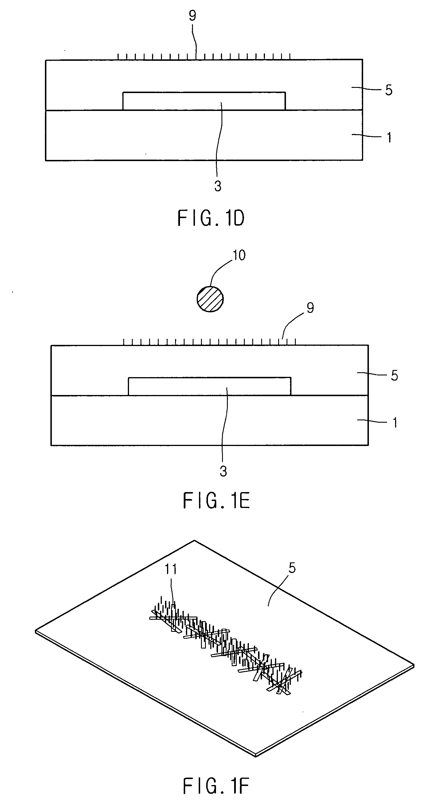
[0029]As illustrated in FIG. 1C, a self-assembled monolayer (SAM) material having a charge of a first polarity and an —NH2 group forms a SAM layer 9 on the substrate 1 having the photoresist pattern 7 through a gas reaction. The charge of the first polarity may be positive. The SAM layer 9 with a positive charge can pull a material having a negative charge and maintain a ...

second embodiment

[0044]FIGS. 2A to 2E are views of manufacturing processes of a liquid crystal display device with a thin film transistor according to a

[0045]The thin film transistor of FIGS. 2A to 2E may be manufactured using the same method as that of FIGS. 1A to 1H.

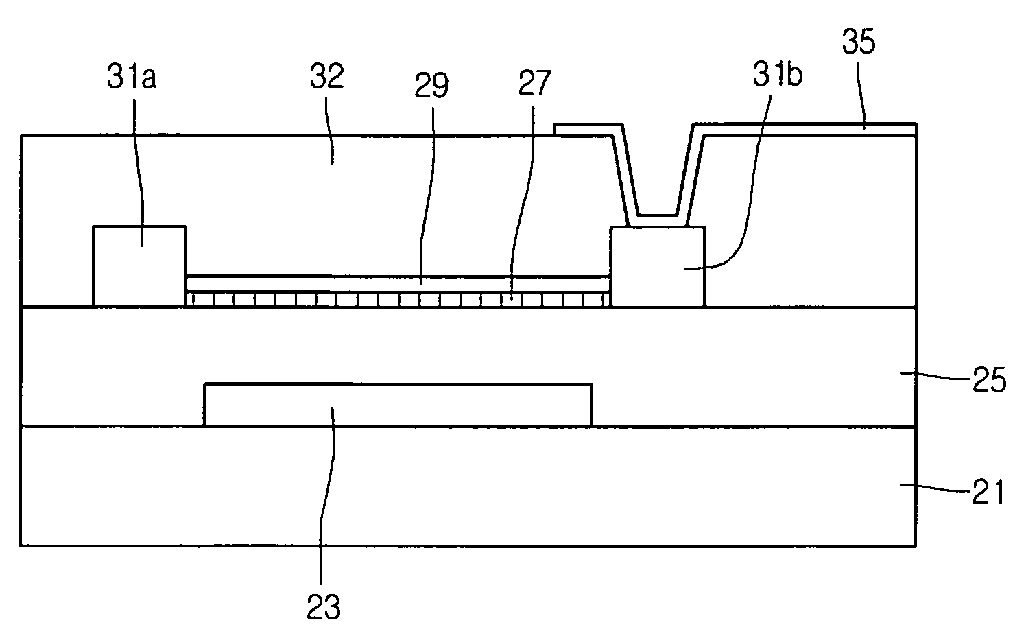
[0046]As illustrated in FIG. 2A, a first metal layer is deposited on a substrate 21, and then is patterned to form a gate electrode 23 and a gate line. The first metal layer may include a least one of Cu, Al, AlNd, Mo, Cr, Ti, Ta, and MoW.

[0047]A gate insulating layer 25 having an inorganic material such as SiNx and SiOx is formed on the substrate 21 having the gate electrode 23.

[0048]As illustrated in FIG. 2B, a semiconductor layer is formed using nanowires 29.

[0049]More specifically, a photoresist material is deposited on the gate insulting layer 25 first, and then is expose to uncover the gate insulating layer 25 corresponding to the semiconductor layer, such that a photoresist pattern (not shown) is formed.

[0050]A SAM material is f...

third embodiment

[0060]FIGS. 3A to 3H are views of manufacturing processes of a thin film transistor according to a

[0061]The second embodiment is similar to the first embodiment. Accordingly, processes similar to those of the first embodiment will be briefly described in the description of the second embodiment.

[0062]As illustrated in FIG. 3A, a first metal layer is deposited on the substrate 1, and then patterned to form a gate electrode 3.

[0063]Next, an insulating material is deposited on the substrate 1 having the gate electrode 3 to form a gate insulating layer 5.

[0064]As illustrated in FIG. 3B, a SAM material having a charge of a first polarity and an —NH2 group forms a SAM layer 51 on the gate insulating layer 5 through a gas reaction. The charge of the first polarity may be positive.

[0065]As illustrated in FIG. 3C, after a mask 53 is arranged, a deep-ultraviolet (UV) irradiation is projected on the SAM layer 51.

[0066]As illustrated in FIG. 3D, the SAM layer 51 where the deep-UV is blocked by ...


PUM


Abstract

A method of manufacturing a thin film transistor includes: forming a gate insulating layer on a substrate having a gate electrode; forming a semiconductor layer of nanomaterial on the gate insulating layer; forming a source electrode and a drain electrode on the gate insulating layer; and applying a voltage to the source electrode and the drain electrode to arrange a direction of the nanomaterial.

Description

[0001]This application claims the benefit of Korean Patent Application No. 2006-0124387 filed on Dec. 8, 2006, which is hereby incorporated by reference for all purposes as if fully set forth herein.BACKGROUND OF THE INVENTION[0002]1. Field of the Invention[0003]The present disclosure relates to a thin film transistor, and more particularly, to a method of manufacturing a thin film transistor including a nanomaterial and a method of manufacturing a liquid crystal display device using the same.[0004]2. Discussion of the Related Art[0005]Recently, research for utilizing a nanomaterial such as a nanowire, a carbon nanotube, and a nanocable is actively under development. Therefore, a semiconductor layer can be formed of the nanomaterial.[0006]The nanomaterial itself is formed of a crystal, such that its electron mobility is almost identical to that of a metal oxide semiconductor field effect transistor (MOSFET).[0007]In the case where a thin film transistor is manufactured using the nan...

Claims


Application Information

Patent Timeline
IPC IPC(8): H01L21/02H01L29/786
CPCB82Y10/00H01L29/66742H01L29/0673H01L29/0665G02F1/136B82Y30/00
Inventor LEE, BO HYUNMOON, TAE HYOUNG
Owner LG DISPLAY CO LTD
Why Eureka
Try Eureka