

Precursors for the deposition of carbon-doped silicon nitride or silicon oxynitride films
a technology of silicon oxynitride and precursors, which is applied in the direction of coatings, chemical vapor deposition coatings, metallic material coating processes, etc., can solve the problems of plasma charging damage, relative high cost and difficulty in etching, and low silicon nitride or silicon oxynitride deposition
- Summary
- Abstract
- Description
- Claims
- Application Information
AI Technical Summary
Problems solved by technology
Method used
Image

Examples
Embodiment Construction
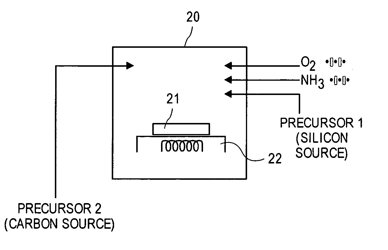
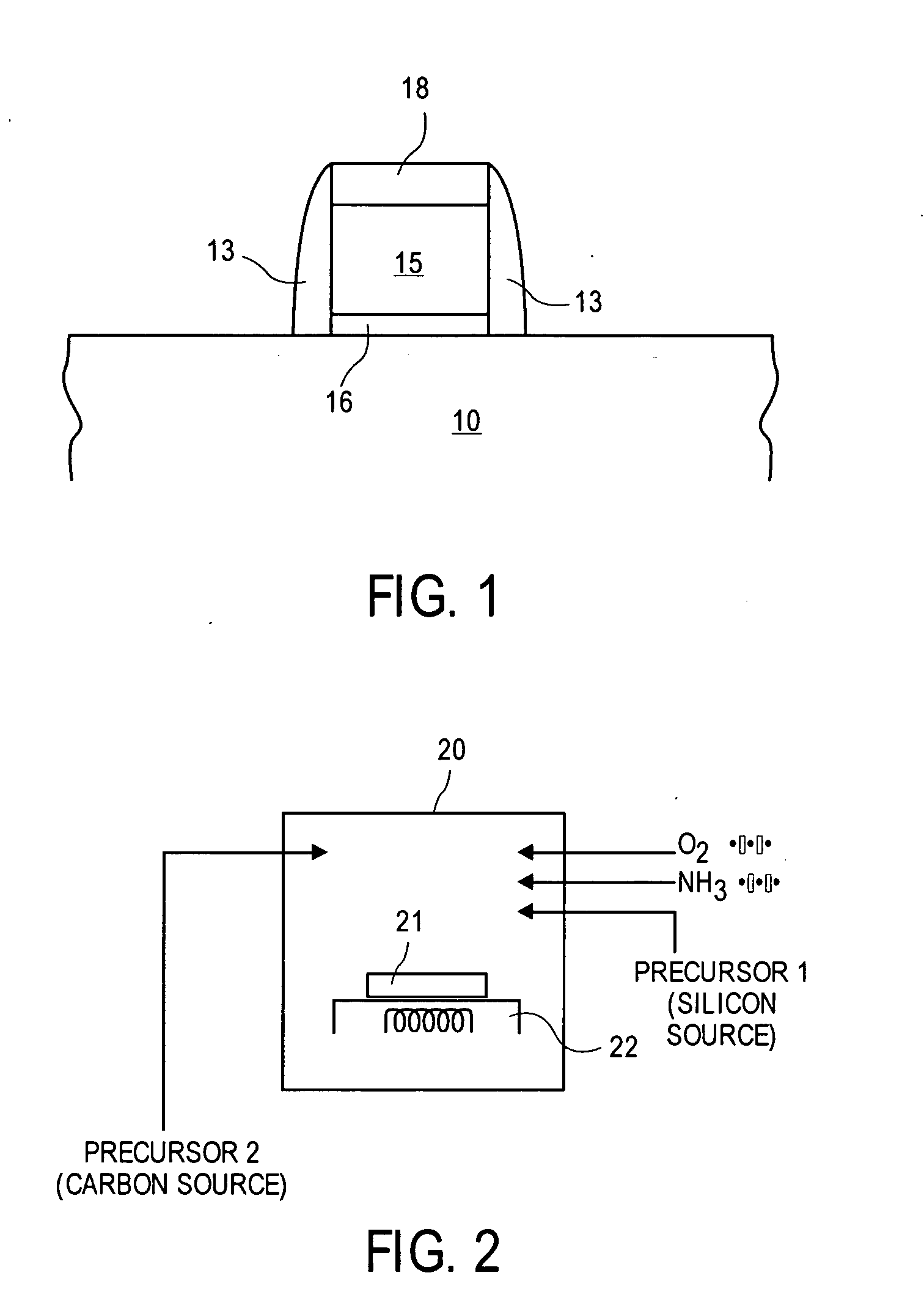
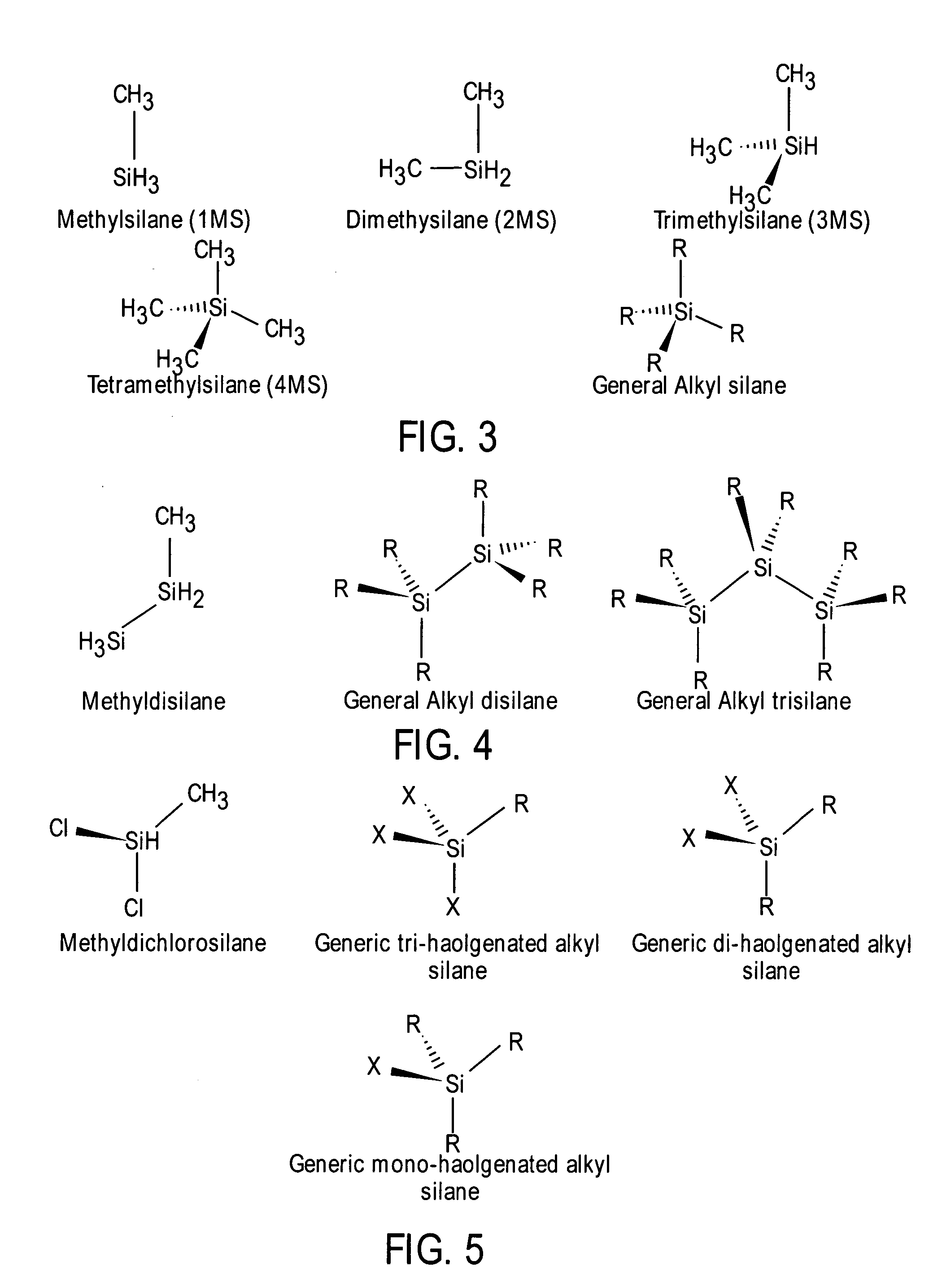
[0014] A method for fabricating insulative regions and their use in an integrated circuit is described. In the following description, numerous specific details such as specific precursors are described in order to provide a thorough understanding of the present invention. It will be apparent to one skilled in the art that the present invention may be practiced without these specific details. In other instances, well-known processes, etchants and deposition techniques are not described in detail in order not to unnecessarily obscure the present invention.
[0015] As mentioned earlier, silicon nitride films and silicon nitride films with oxygen, referred to as silicon oxynitride films, are prominently used in the fabrication of semiconductor devices, particularly integrated circuits. These materials exhibit the characteristics of a refractory material, have a relatively high dielectric constant (e.g., 6-8), have a relatively low coefficient of thermal expansion, and are an excellent di...
PUM
| Property | Measurement | Unit |
|---|---|---|
| semiconductor | aaaaa | aaaaa |
| melting point | aaaaa | aaaaa |
| electrical | aaaaa | aaaaa |
Abstract
Description
Claims
Application Information