Semiconductor device having resin-sealed area on circuit board thereof

a semiconductor device and resin-sealed technology, applied in the direction of semiconductor devices, semiconductor/solid-state device details, electrical apparatus, etc., can solve the problem of increasing the cost of the semiconductor device attributable to the additional step, affecting the step, and the leakage of resin cannot be effectively prevented, so as to prevent the occurrence of poor connection of solder balls

Inactive Publication Date: 2006-10-19
RENESAS ELECTRONICS CORP
View PDF42 Cites 9 Cited by
  • Summary
  • Abstract
  • Description
  • Claims
  • Application Information

AI Technical Summary

Benefits of technology

[0014] Accordingly, it is an object of the present invention to provide a semiconductor device that permits easy manufacture of a semiconductor device having a sealing resin molded to seal a semiconductor chip onto a circuit board, and that reduces resin burrs caused by leakage of a sealing resin and also restrains the occurrence of disconnection attributable to a crushed wiring layer.
[0019] In the present invention, the interval dimension between the adjacent ones of the plurality of wiring patterns ranges from 50% to 200%. Hence, between the wiring patterns, no gap will be produced between a clamping portion of a metal mold applied to a circuit board and the front surface of the circuit board when molding a sealing resin onto the front surface of the circuit board. Therefore, when a sealing resin is injected into the cavity of the metal mold to mold the sealing resin, no major resin leakage will result, thus restraining the occurrence of poor connection of solder balls or disconnection of wiring layers. In addition, when a load is applied to the wiring patterns in a molding line area by the clamping force of the metal mold, the load is applied such that it is evenly scattered to the individual wiring patterns, thus preventing the wiring patterns from being crushed and disconnected by the metal mold.

Problems solved by technology

Regarding these BGA type semiconductor devices, a problem is described in that a molding resin runs off through a gap between a metal mold and a wiring board in the vicinity of a visible outline (molding line) of a molding resin layer in the peripheral portion of the circuit board, and resin burrs occur, adversely affecting the step for cutting the circuit board to for each semiconductor device.
However, the art in which the laminated solder resist or the dam frame is formed to close the gap between the circuit board and the metal mold requires the step for forming such a laminated solder resist or dam frame, leading to increased cost of the semiconductor device attributable to the additional step.
Furthermore, unless the laminated solder resist or the dam frame is formed along the molding line of a sealing resin, the leakage of a resin cannot be effectively prevented.
A smaller semiconductor device, in particular, requires high positioning accuracy, making it more difficult to fabricate the semiconductor device and also making the manufacturing process more complicated.
The conventional ABGA type semiconductor device set forth has been posing the following problems.
Thus, the conventional ABGA type semiconductor device as been presenting a problem in that defects such as poor connection of the solder balls, the disconnection of the wiring layer, or the like takes place, resulting in a lower manufacturing yield of the semiconductor devices and degraded reliability of the semiconductor devices.
Accordingly, the circuit board having the solder resist 415 with the uneven surface due to the uneven density of the wiring patterns poses the problem described below when sealing the semiconductor chip or the like mounted thereon by a sealing resin.
There is another problem.
This leads to an increase in the electrical resistance or disconnected wiring patterns in some cases.

Method used


Image

  • Semiconductor device having resin-sealed area on circuit board thereof
  • Semiconductor device having resin-sealed area on circuit board thereof
  • Semiconductor device having resin-sealed area on circuit board thereof

Examples


first embodiment

[0037] Referring to the accompanying drawings, the present invention will be explained in detail.

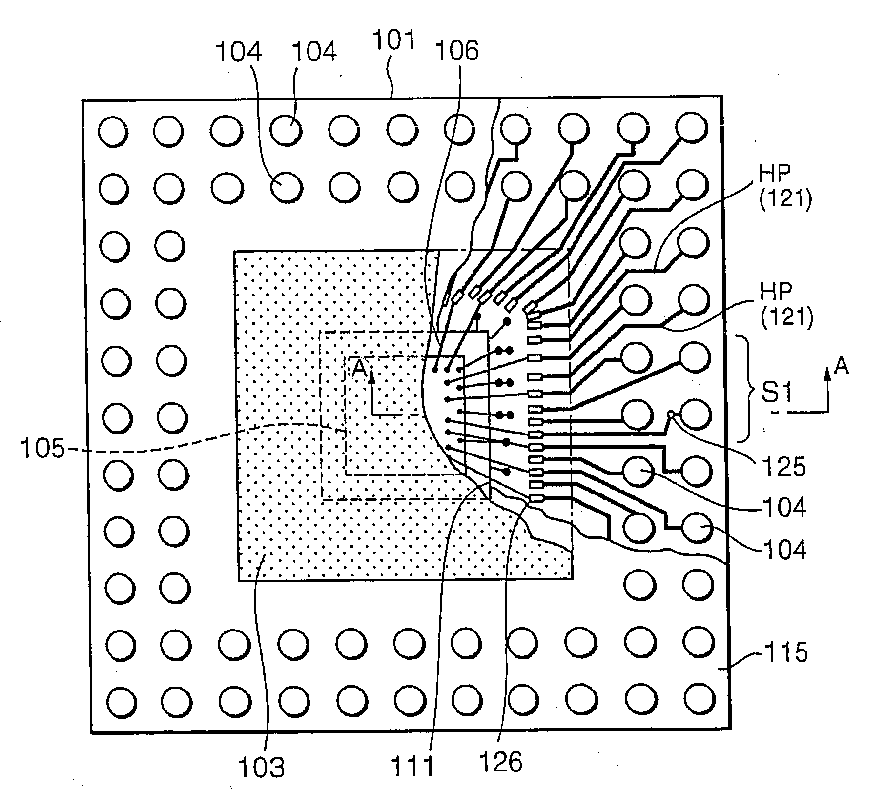
[0038]FIG. 7 is a schematic perspective view of an embodiment in which the present invention has been applied to an ABGA type semiconductor device; FIG. 8 is a plan view of the semiconductor device with a part of a sealing resin cut away; FIG. 9 is an enlarged plan view of an essential area S1 shown in FIG. 8; FIG. 10 is an enlarged sectional view taken at the line A-A shown in FIG. 8; and FIG. 11 is an enlarged sectional view wherein a part along the line B-B shown in FIG. 9 has been omitted.

[0039] Referring to FIG. 7, the ABGA type semiconductor device has a heat spreader 102 integrally attached to the bottom surface of a circuit board 101, the heat spreader 102 being constructed of a metal plate having high thermal conductivity. A molded sealing resin 103 is provided in the central area of the circuit board 102 to seal a semiconductor chip or the like, which will be discussed hereina...

third embodiment

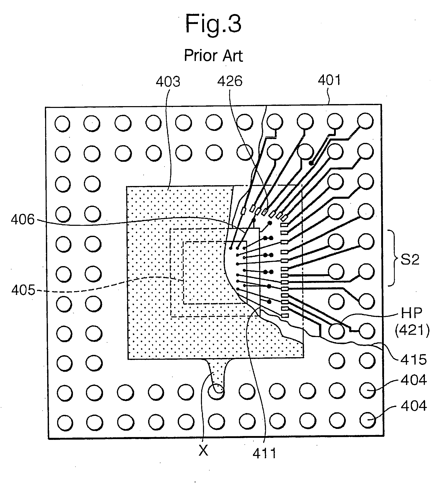
[0049] A third embodiment in accordance with the present invention will be described in detail with reference to relevant drawings. Referring to FIG. 13, the density of wiring patterns HP is low in the area wherein the number of the wiring patterns HP per unit area is small, as in the four-side area of the circuit board 101, and it is difficult to dispose the wiring patterns HP at the aforesaid interval dimension d. For this reason, a dummy wiring pattern DHP is formed between the wiring patterns HP so as to set the interval dimension d between the dummy wiring pattern DHP and the wiring pattern HP to 50% to 200% of an adjacent wiring interval at least in the molding line area MLA.

[0050] The dummy wiring patterns DHP are electrically connected to a power wiring layer of the third wiring layer 123 or a ground wiring layer or the like of the fourth wiring layer 124 via the through holes 126 to maintain a fixed potential state. The dummy wiring pattern DHP may be formed to be a wiring ...


PUM


Abstract

A semiconductor device having a molded sealing resin for sealing a semiconductor chip on a circuit board thereof reduces resin burrs resulting from the leakage of the sealing resin, and also restrains the occurrence of disconnection caused by a wiring layer being crushed. In the semiconductor device, the sealing resin for sealing the semiconductor chip is molded on the circuit board that has a plurality of wiring patterns and a solder resist for insulatively covering the wiring patterns formed on the front surface thereof, the interval of the wiring patterns is set to range from 50% to 200% of its adjacent interval in a molding line area of the sealing resin.

Description

BACKGROUND OF THE INVENTION [0001] 1. Field of the Invention [0002] The present invention relates to a semiconductor device in which the surface of a circuit board thereof is resin-sealed together with a semiconductor chip thereof and, more particularly, to a semiconductor device that restrains degradation of the reliability of the semiconductor device by resin sealing. [0003] 2. Description of the Related Art [0004] With the trend toward a thinner semiconductor device with more pins, there has been proposed a semiconductor device having a ball grid array (BGA) structure (hereinafter referred to as the “BGA type semiconductor device”). In the BGA type semiconductor device, a semiconductor chip is mounted on a circuit board, and solder balls provided on the circuit board serve as external connection terminals. This arrangement makes it possible to control the thickness of the package to about the thickness of the circuit board and to allow numerous solder balls to be arranged at high...

Claims


Application Information

Patent Timeline
Patent Type & Authority Applications(United States)
IPC IPC(8): H01L23/02H01L21/56H01L23/28H01L23/12
CPCH01L24/49H01L2224/48227H01L2924/014H01L2924/01033H01L2224/48228H01L2224/49171H01L2224/4943H01L2924/01004H01L2924/01005H01L2924/01006H01L2924/0102H01L2924/01082H01L2924/15153H01L2924/1517H01L2924/15311H01L2924/1532H01L21/565H01L2924/00H01L2924/181H01L2924/00014H01L24/48H01L2224/49431H01L2224/45099H01L2224/05599H01L2924/00012
Inventor MATSUDA, SHUICHI
Owner RENESAS ELECTRONICS CORP
Why Eureka
Try Eureka