Multilayer printed wiring board

a wiring board and multi-layer technology, applied in the association of printed circuit non-printed electric components, electrical apparatus construction details, semiconductor/solid-state device details, etc., can solve the problems of inability to inspect ic chips or substrates, inability to repair layered ic chips, and inability to use loaded substrates themselves, etc., to achieve the effect of applying the most effective

Active Publication Date: 2006-10-26
IBIDEN CO LTD
View PDF14 Cites 110 Cited by
  • Summary
  • Abstract
  • Description
  • Claims
  • Application Information

AI Technical Summary

Benefits of technology

[0116] The thickness of the protective film is preferred to be in a range of 0.01-3 μm. The reason is that if it is less than 0.01 μm, fine unevenness of the mat face cannot be covered completely and if it exceeds 3 μm, the protective film is loaded in the concave portions in the formed mat face, thereby mat treatment e...

Problems solved by technology

However, the substrate loaded with the layered IC chips cannot be repaired.
Further, because connection is gained by wire bonding after the loading, the IC chip or the substrate cannot be inspected until the connection is gaine...

Method used


Image

  • Multilayer printed wiring board
  • Multilayer printed wiring board
  • Multilayer printed wiring board

Examples


embodiments

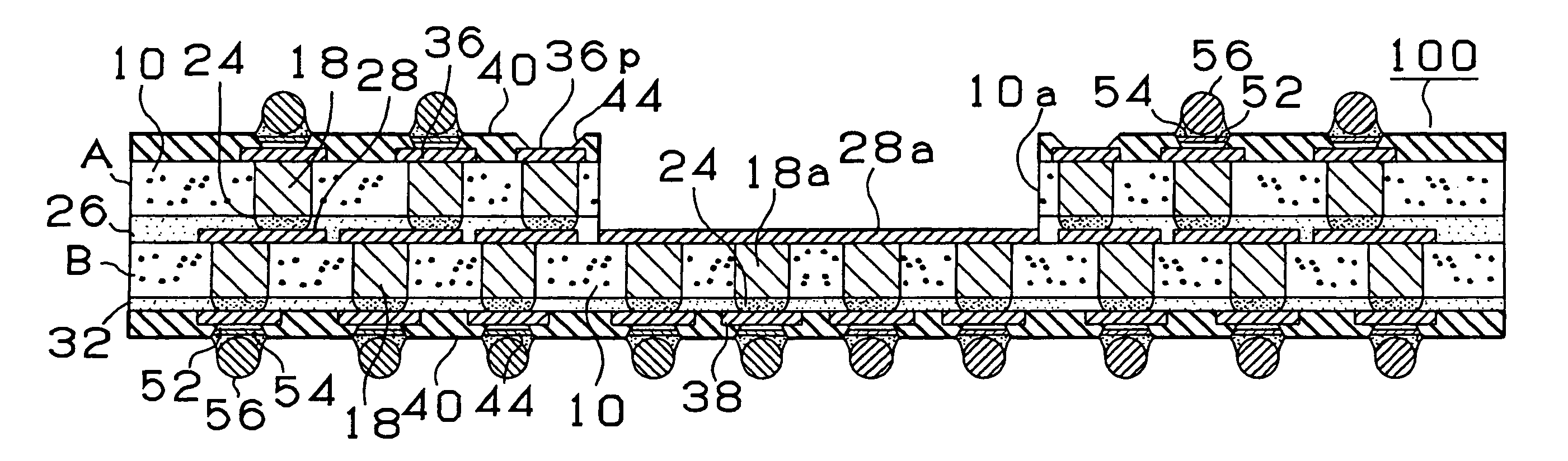
[0149] First, the structure of the multi-layer printed wiring board in which the single side circuit boards are multi-layered according to the first embodiment of the present invention will be described with reference to FIGS. 1, 2.

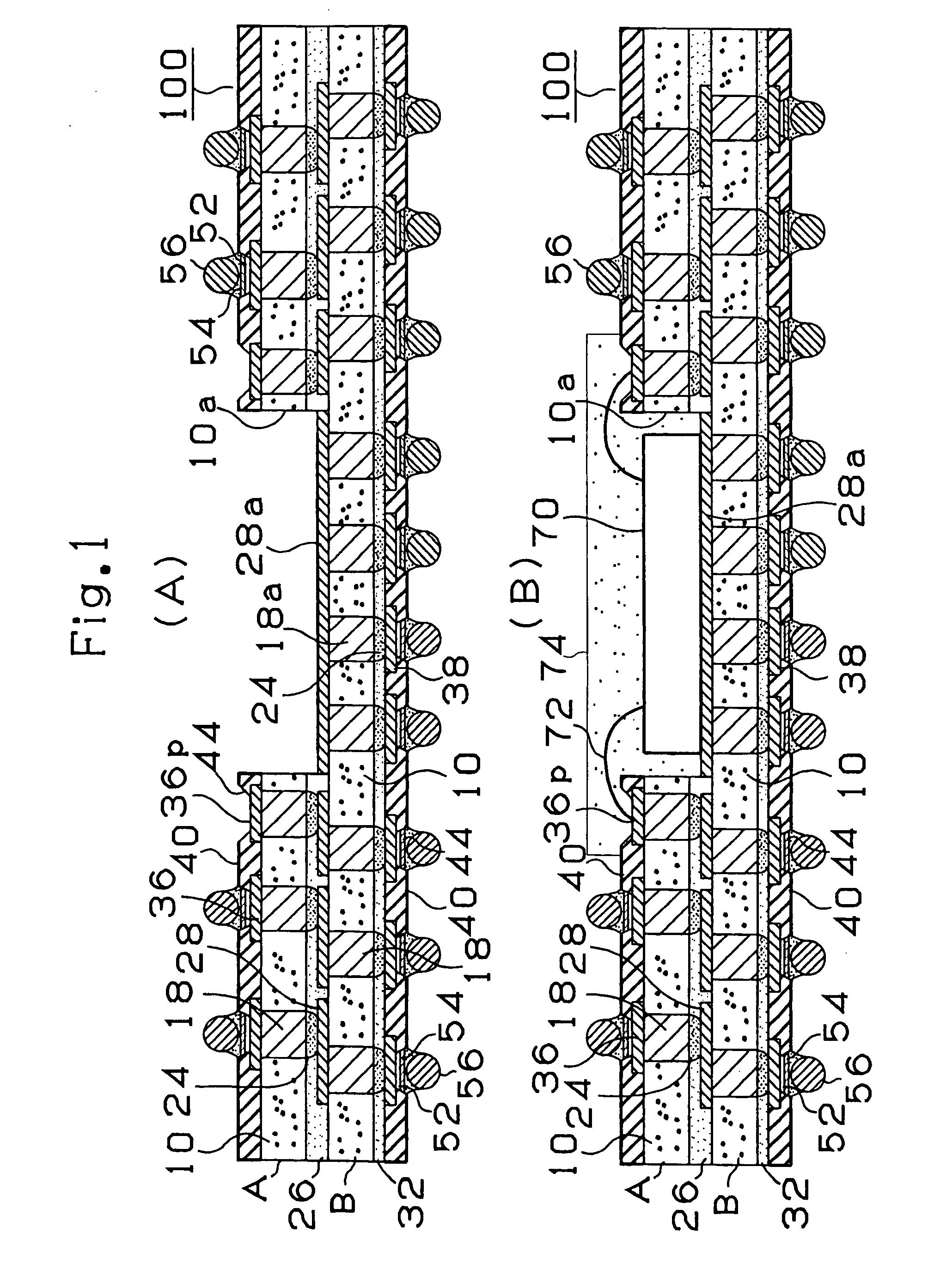
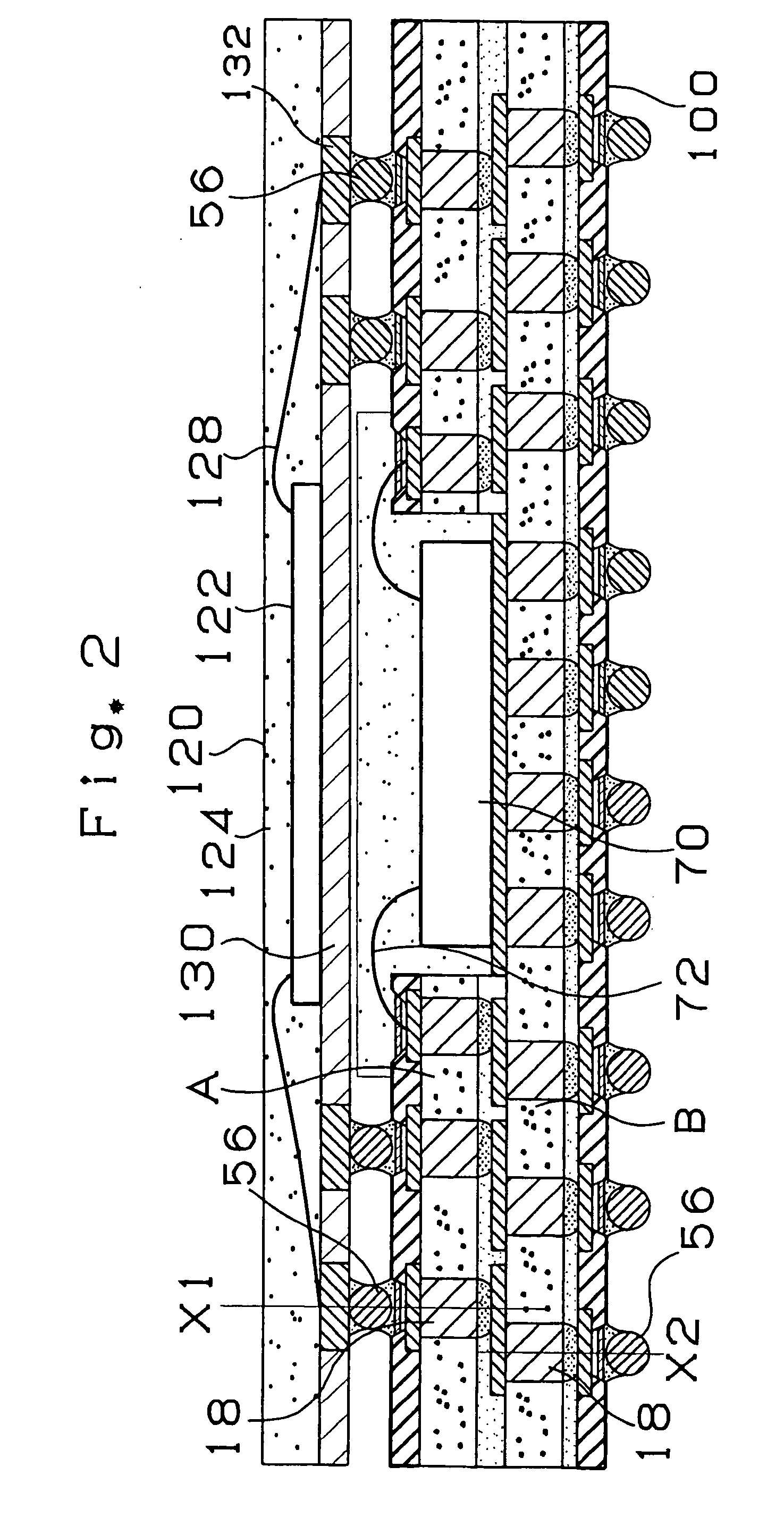
[0150]FIG. 1 shows the structure of the multi-layer printed wiring board 100 constituting a package substrate and FIG. 1(B) shows a condition in which an IC chip 70 is mounted on the multi-layer printed wiring board 100. FIG. 2 shows a condition in which an IC module 120 is mounted on the multi-layer printed wiring board 100 loaded with the IC chip 70.

[0151] As shown in FIG. 1(A), the multi-layer printed wiring board 100 is produced by stacking a single side circuit board A of two layers and a single side circuit board B. An opening (bored portion) 10a for accommodating the IC chip is formed in the center of the upper single side circuit board A. A conductor circuit 36 is formed on the top face of the single side circuit board A and a BGA 56 for connect...

example 1

[0221] (1) First, a single side circuit board constituting a multi-layer printed wiring board is produced. For this circuit board, a single side copper stretched layered board obtained by overlaying a prepreg as B stage in which epoxy resin is impregnated with glass cloth and copper foil and then pressing them with heat is used as a starting material.

[0222] This insulating base material is 75 μm thick and the copper foil is 18 μm thick. The surface on an opposite side to the copper foil forming face of this layered board is laminated with PET film 12 μm thick and having adhesive agent layer 12 μm thick.

[0223] (2) Next, by irradiating the PET film with carbon dioxide laser, a via hole forming opening going through the PET film and insulating base material up to the copper foil is made and further it is permissible to de-smear the inside of the opening by oxygen plasma discharge or dipping in chemical solution of acid, oxidizing agent or alkali. By the de-smear treatment, the base m...

second embodiment

[0259] First, the structure of a multi-layer printed wiring board produced by overlaying the single side circuit boards, according to the second embodiment of the present invention will be described with reference to FIGS. 17, 18.

[0260]FIG. 17(A) shows a multi-layer printed wiring board 100 constituting a package board and FIG. 17(B) shows a condition in which the IC chip 70 is mounted on the multi-layer printed wiring board 100. FIG. 18(A) shows a condition in which the IC chip 70 of the multi-layer printed wiring board shown in FIG. 17(A) is molded with resin and FIG. 18(B) shows a condition in which the IC module 120 is mounted on the multi-layer printed wiring board 100 loaded with the IC chip 70.

[0261] As shown in FIG. 17(A), the multi-layer printed wiring board 100 comprises two layers, the single side circuit board A and the single side circuit board B. The top face of the single side circuit board A and the bottom face of the single side circuit board B are covered with so...


PUM


Abstract

In a multi-layer printed wiring board 100 comprising single side circuit boards A, B and for accommodating an IC chip 70, BGAs 56 are disposed on its front and rear faces, so that with an IC module 120 mounted through the BGA 56 on the front face, this board can be connected to a printed wiring board through the BGA 56 on the rear face. Thus, freedom in the configuration of the IC module mounted increases so that various kinds of the IC modules can be loaded.

Description

TECHNICAL FIELD [0001] The present invention relates to a multi-layer printed wiring board loaded with electronic components such as IC chips and more particularly to a multi-layer printed wiring board which enables the IC chip to be multi-layered and is not affected by stress and the like. BACKGROUND ART [0002] Technology which multi-layers an insulation substrate having IVH (inner via hole) structure while equipped with a conductive layer on one side has been proposed (for example, Japanese Patent Application Laid-Open No. HEI10-13028 and the like). This makes electric connection by connecting the conductive layer of one insulating base material with the via hole in the other insulating base material. Its function is exerted by mounting electric components such as IC chip and capacitor on a conductor circuit on an external layer appropriately. As a conventional art, Japanese Patent Application Laid-Open No. HEI10-13028 has been known. [0003]FIG. 24 shows a printed wiring board for...

Claims


Application Information

Patent Timeline
IPC IPC(8): H05K1/11H05K1/18H01L23/498H01L25/10H05K1/14H05K3/46
CPCH01L23/49827H01L23/49838H01L24/06H01L24/49H01L25/105H01L2224/32145H01L2224/48091H01L2224/48227H01L2224/48228H01L2224/48235H01L2224/49171H01L2224/4943H01L2924/01005H01L2924/01006H01L2924/01011H01L2924/01013H01L2924/01015H01L2924/01028H01L2924/01029H01L2924/0103H01L2924/01033H01L2924/01047H01L2924/01049H01L2924/0105H01L2924/01051H01L2924/01075H01L2924/01078H01L2924/01079H01L2924/01082H01L2924/01083H01L2924/014H01L2924/14H01L2924/15153H01L2924/15165H01L2924/1517H01L2924/15311H01L2924/15331H01L2924/19041H01L2924/30107H05K1/0206H05K1/113H05K1/144H05K1/183H05K3/4614H05K3/4617H05K3/4652H05K2201/0355H05K2201/0394H05K2201/09627H05K2203/049H05K2203/0733H01L24/48H01L2924/01019H01L2924/3511H01L2224/32225H01L2224/73265H01L2225/1058H01L2224/04042H01L2225/1023H01L2224/05554H01L2924/00014H01L2924/00012H01L2924/12042H01L24/73H01L2924/181H01L2224/49431H01L2224/49433H01L2924/10162H01L2224/45099H01L2224/05599H01L2924/00
Inventor KARIYA, TAKASHITSUDA, AKIYOSHI
Owner IBIDEN CO LTD
Why Eureka
Try Eureka