
Display Device and Semiconductor Device

a display device and semiconductor technology, applied in semiconductor devices, instruments, electrical equipment, etc., can solve the problems of increasing the cost of the driver ic, increasing the power consumption, and increasing the power consumption with a rise in the operating speed, so as to reduce the noise level of the emi and reduce the cost. , the effect of reducing the cos

Active Publication Date: 2006-10-26
HANNSTAR DISPLAY CORPORATION
View PDF22 Cites 6 Cited by
  • Summary
  • Abstract
  • Description
  • Claims
  • Application Information

AI Technical Summary

Benefits of technology

The present invention provides a display device that can achieve high-definition, multicolor display at lower cost and with reduced power consumption. The invention also addresses the problem of limited reliability in display devices caused by high-speed operation. The invention solves these problems by reducing the cost and power consumption of the driver circuit, simplifying the fabrication process, reducing the number of pixels and tones, suppressing the effects of EMI, and improving the reliability of the display device. The invention also provides a display panel with a reduced number of bus lines for data transfer, which reduces the operating frequency of the data-line driver circuit and allows for the use of a single process for manufacturing the transistor elements in the peripheral circuits. The invention also includes a display memory and a DAC for converting display data to an analog signal, which further reduces power consumption and improves reliability.

Problems solved by technology

The conventional display device set forth above has a number of problems.
A first problem is that an increase in the cost of the driver IC and an increase in power consumption accompany an improvement in definition and tonality of the display.
As a result of high-speed data transfer, the driver IC also is required to exhibit high speed, short circuit current from a higher potential power supply to a lower potential power supply is produced in the large number of CMOS elements that constitute the circuit elements, and therefore power consumption increases with a rise in operating speed.
Further, an IC that operates at high speed also is high in price.
When there is an increase in the number of tones, this necessitates more complicated circuitry and even higher transfer speed, thereby inviting greater power consumption and higher cost.
This also leads to an increase in cost.
A second problem is that a limitation is imposed upon the number of pixels and the number of tones (gray-scales) owing to the need to suppress the overall power consumption and price of the system.

Method used


Image

  • Display Device and Semiconductor Device
  • Display Device and Semiconductor Device
  • Display Device and Semiconductor Device

Examples


12th embodiment

[0198] A 12th embodiment of the present invention will now be described with reference to FIG. 18, which illustrates the structure of a display device according to this embodiment.

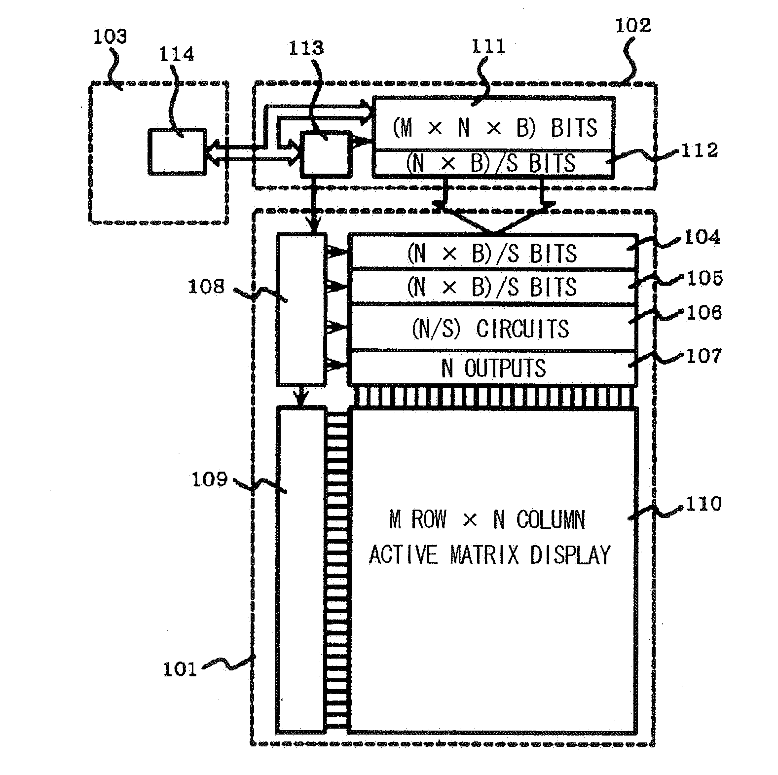
[0199] As shown in FIG. 18, the 12th embodiment includes the circuit board 103 on the system side, the controller IC 102 and the display device substrate 101. The circuit board 103 on the system side includes the interface circuit 114 by which the board is connected to the controller IC 102. The controller IC 102 includes the controller 113, the memory 111 and the output buffer 112 and is connected to the system circuit board 103 and to the display device substrate 101.

[0200] The display device substrate 101 has, built in, the level shifter / timing buffer 108, scanning circuit 109, level shifter 104, latch circuit 105, DAC 106, selector circuit 107, serial / parallel converting circuit 1801 and display area 110 and is connected to the controller IC 102. The level shifter 104, serial / parallel converting circ...

15th embodiment

[0224] A 15th embodiment of the present invention will now be described with reference to FIG. 22, which illustrates the structure of a display device according to this embodiment.

[0225] As shown in FIG. 22, the 15th embodiment includes the circuit board 103 on the system side, the controller IC 102 and the display device substrate 101. The circuit board 103 on the system side includes the interface circuit 114 by which the board is connected to the controller IC 102. The controller IC 102 includes the controller 113, the memory 111 and the output buffer 112 and is connected to the system circuit board 103 and to the display device substrate 101.

[0226] The display device substrate 101 has, built in, the timing buffer 401, scanning circuit 109, latch circuit 105, DAC 106, selector circuit 107, serial / parallel converting circuit 1801 and display area 110 and is connected to the controller IC 102. The serial / parallel converting circuit 1801, latches circuit 105, level shifter 104 and...

16th embodiment

[0230] A 16th embodiment of the present invention will now be described with reference to FIG. 23, which illustrates the structure of a display device according to this embodiment.

[0231] As shown in FIG. 23, the 16th embodiment includes the circuit board 103 on the system side, the controller IC 102 and the display device substrate 101. The circuit board 103 on the system side includes the interface circuit 114 by which the board is connected to the controller IC 102. The controller IC 102 includes the controller 113, the memory 111 and the output buffer 112 and is connected to the system circuit board 103 and to the display device substrate 101.

[0232] The display device substrate 101 has, built in, the level shifter / timing buffer 108, scanning circuit 109, level shifter 104, latch circuit 105, DAC 106, selector circuit 107, serial / parallel converting circuit 1801, voltage-current converting circuit / current output buffer 801 and display area 110 and is connected to the controller ...


PUM


Abstract

A display device of high definition, multiple colors and low power consumption includes a display panel having a pixel section in which pixels are arrayed in the form of a matrix at the cross points of a plurality of data lines and a plurality of scanning lines, a scanning circuit for applying voltage sequentially to the plurality of scanning lines, and a data-line driver, which receives display data supplied by a host device, for applying signals corresponding to the display data to the plurality of data lines. Provided external to the display panel is a controller IC having a display memory for storing display data corresponding to the pixel section, an output buffer for reading data out of the display memory and outputting this data to the display panel, and a controller for controlling the display memory and output buffer and communication with the host device. The display panel is provided with a digital / analog converter, which forms part of the data-line driver, for converting display data represented by a digital signal to an analog signal. The width of a bus for data transfer between the controller IC and data-line driver of the display panel is such that data of a greater number of bits is transferred in parallel by a single transfer than is transferred by the bus between the controller and the host device. This allows the operating frequency of the data-line driver to be reduced.

Description

[0001] This is a divisional of application Ser. No. 10 / 261,584 filed Oct. 2, 2002. The entire disclosure of the prior application, application Ser. No. 10 / 261,584 is hereby incorporated by reference.FIELD OF THE INVENTION [0002] This invention relates to a display device used in a projector, a notebook personal computer, a monitor, a cellular phone and a personal digital assistant, etc. More particularly, the invention relates to a voltage-driven display device and current-driven display device such as a liquid crystal display device. BACKGROUND OF THE INVENTION [0003] As the era of multimedia has progressed, so has the rapid spread of display devices. These find use in small-size applications such as the viewfinders of projectors and video cameras as well as cellular phones, in mid-size applications such as the display panels of vehicular televisions and navigation systems as well as mobile terminals such as personal digital assistants (PDAs) and pocket personal computers, and in l...

Claims


Application Information

Patent Timeline
Patent Type & Authority Applications(United States)
IPC IPC(8): H01L29/04G09G3/20G09G3/36G09G5/00
CPCG09G3/2011G09G3/3648G09G3/3688G09G5/006G09G2300/0408G09G2300/08G09G2370/08G09G2310/0275G09G2310/0289G09G2310/0297G09G2310/06G09G2330/021G09G2330/06G09G2310/027
Inventor HAGA, HIROSHITAKATORI, KENICHIASADA, HIDEKI
Owner HANNSTAR DISPLAY CORPORATION
Learn More